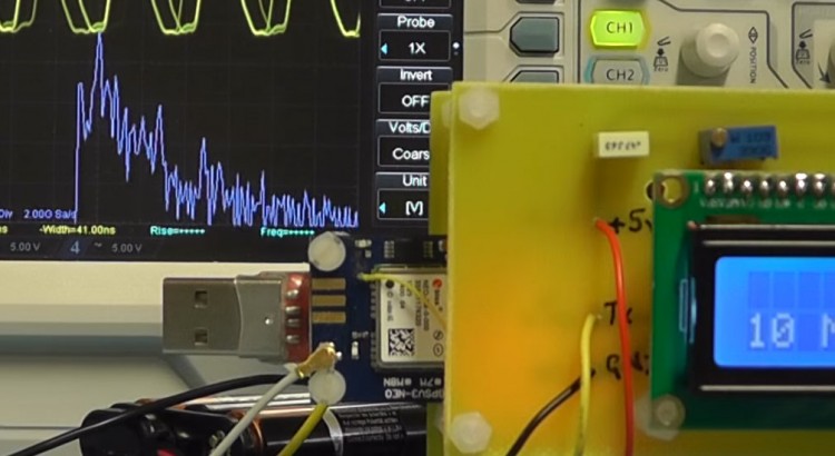
In Part 2 of this project we will improve the reception of the GPS module and build the project on to printed circuit boards and test the unit. In addition we will look at ways of converting the 10MHz square wave to a sine wave.
Below are links to download the schematics and PCB layouts for both the Main Frequency PCB and the Display PCB also the parts list.
Frequency reference – I’ve tried two browsers but it seems the posted video for Part 2 is in fact the video for Part 1?