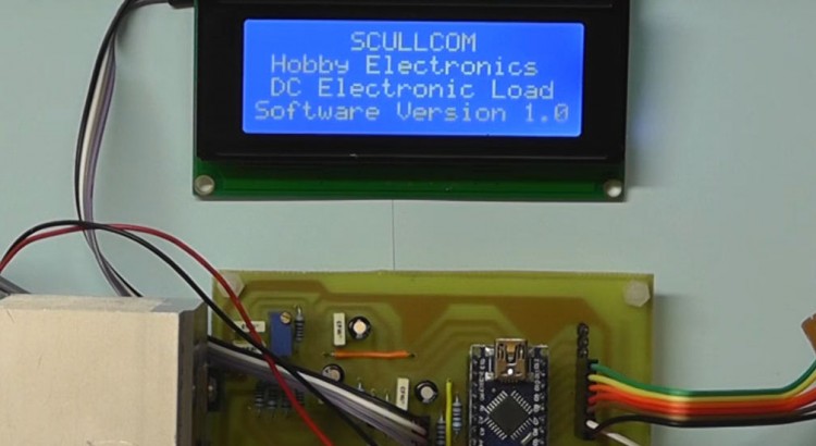
In this project we will design an build an Electronic DC Load which is capable of Constant Current, Constant Power and Constant Resistance. The design will use a rotary encoder for input entry and a 20×4 LCD display as the user interface. In Part 1 of this project we will discuss the basic design and then build and test the initial prototype.
Below are links for the prototype software plus a zip file with the schematic, PCB artwork and component layout:
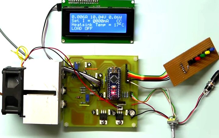
Above shows the PCB wired for testing with heatsink and fan added.
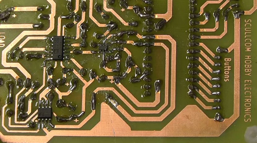
Underside of PCB showing the locations of the 3 IC’s.
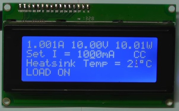
Close up of 20×4 LCD showing setting in Constant Current Mode.
PART 2
In part 2 of this project we will make some changes in the way the LCD displays the information. The set current and set power levels are now set in Amps and Watts to three decimal places. Safety limits have also been added to limit maximum current setting and maximum power. After start up the unit goes in to constant current mode. A battery capacity function has also been added to test the life of batteries in mAh. The power mosfet has now been changed to a BUK956R1-100E (from NXP) to improve power handling. Finally software has been upgraded to Version 2.0.
Below are links to the downloads for Part 2 of this project:
http://www.scullcom.com/Electronic_Load_software_V2.0.ino
http://www.scullcom.com/MCP79410Timer-master.zip
http://www.scullcom.com/RTC_Module_PCB_Schematic.zip
http://www.scullcom.com/Electronic_Load_Parts_List.pdf
http://www.scullcom.com/DC_Load_Circuit_Part2.pdf
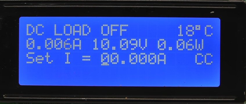
Below is the new LCD layout with the heatsink temperature now at the top left of the display.
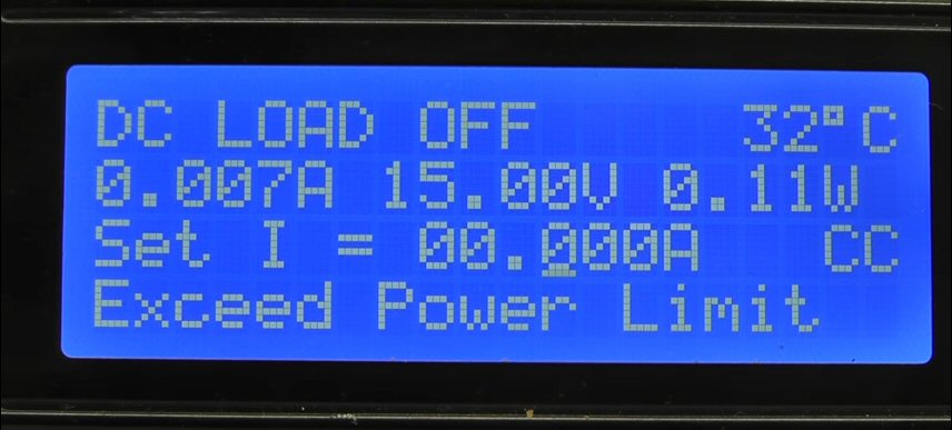
When the power limit is exceeded the Load switches OFF and the display informs “Exceeded Power Limit”.
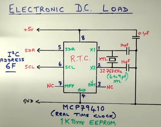
To accommodate the new feature of Battery Capacity Testing we have now added a Real Time Clock (RTC) which also uses the I2C bus to interface with the Arduino.
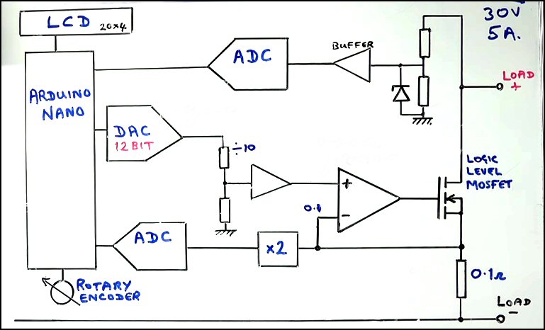
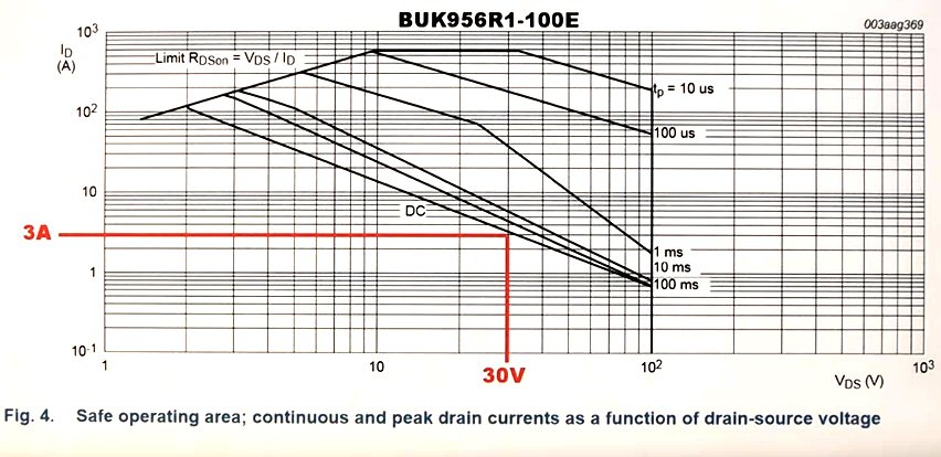
Below is the Safe Operating Area graph, taken from the datasheet, of the Power Mosfet. This illustrates the ability of the Mosfet to handle 3A at 30 volt. However, this is at 25°C and in reality the power handling will be lower than that as the Mosfet heats up. At a later stage we will consider adding Mosfets in parallel to overcome this.
PART 3
In Part 3 of this project we will make a number of improvements and additions. These will include a keypad, improved accuracy, fault protection and enhanced battery capacity discharge test mode. A 4.096 volt reference had been added to the DAC improving accuracy. A battery capacity testing menu has been added.
Below are links to download the latest version of software (version 8) and the updated schematic of the whole project, which now includes Real Time Clock and Voltage Reference Modules:
http://www.scullcom.com/Electronic_Load_software_V8.ino
http://www.scullcom.com/DC_Load_Schematic_ver3.pdf
Please not that the new software now uses a keypad library – ensure that you have the latest version of this library and read the information on the following web page:
http://playground.arduino.cc/Code/Keypad
Direct link for the keypad.h library is below:
http://playground.arduino.cc/uploads/Code/keypad.zip
PART 4
In Part 4 of this project on the Electronic DC Load we are going to add a remote voltage sense circuit, increase the power capacity by adding additional power mosfets and build the completed unit into a metal project case. We will also upgrade the software to allow for input entry via the keypad as well as the rotary encoder.
Below are download links to the latest version of software.
Also a zip file with the updated schematic for the main PCB, schematic and PCB artwork for the Remote Voltage Sense , Parts List, details of alternative power mosfets, wiring diagram and any notes:
http://www.scullcom.com/Electronic_Load_software_V12.ino
http://www.scullcom.com/DC_Load_files_Part4.zip
To increase the Power Cut-Off Level simply change the value in the code below in software:
float PowerCutOff = 50;
Suggest changing 50 to 99
WIRING DIAGRAM LAYOUT LINK BELOW:
http://www.scullcom.com/DC_Load_wiring_layout.pdf
Below is the Remote Sense Circuit which uses a OPA277 OP Amp as a difference amplifier. The negative 5 volt supply for the OP Amp is generated by the a ICL7660 voltage converter IC.
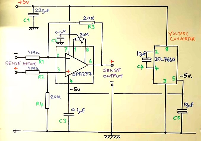
The 20K preset between pins 1 & 8 of the OP Amp is adjusted for a NULL sense output when the sense input terminals are shorted together.
PART 5
In part 5 of this project we will improve the power Mosfet’s current handling capability. Also a Transient Mode will be added providing a pulse option for the DC Load. The software will be updated providing extra features such as; user setting of battery cut-off voltage for battery capacity mode and user setup of safety limits.
Below are links for downloading the latest software and updated schematic diagram:
http://www.scullcom.com/Electronic_Load_software_V24.ino
http://www.scullcom.com/DC_Load_Schematic_v5.pdf
The Remote Voltage Sense circuit remains as show in Part 4 of this project.
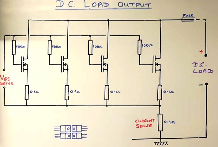
Above is the revised circuit for paralleling the Power Mosfets. Additional 0.1 ohm resistors have been added in the source return of each of the Mosfets so as to reduce the effect of the negative temperature coefficient of the gate/source threshold voltage.
Part 6
In Part 6 of this project we are going to make modifications to the Power Mosfet drive circuit to improve the ability to handle higher current/power levels whilst protecting the Mosfets from over heating and possibly going in to thermal runaway. We are also going to design, build and test the trigger input circuit. In addition to this I have updated the software to Version 25.
Below are links to download the latest software. Also there are two zip files providing the PCB artwork, Schematic and Parts List for both the Mosfet Drive Circuit and the Trigger Input Circuit.
http://www.scullcom.com/Electronic_Load_software_V25.ino
http://www.scullcom.com/DC_Load_Mosfet_Drive.zip
http://www.scullcom.com/DC_Load_Trigger_CircuitPCB.zip
IMPORTANT: PLEASE REMEMBER WHEN PRINTING THE PCB ART WORK SET YOUR PRINTER TO PRINT ACTUAL SIZE.
Part 7
In part 7 of this project we will have a look at a number of updates and improvements. We will also use a new single sided PCB with all the components on one board. The Arduino software has also been updated to version 27.
Below are download links to two zip files which provide all the details. One for the updates, schematic, PCB artwork and parts list etc. and another with all the KiCad files. Also a link for the latest software:
http://www.scullcom.com/Electronic_Load_software_V27.ino
http://www.scullcom.com/DC_Load_version7_1.zip
http://www.scullcom.com/DC_Load_v7_1_KiCad_files.zip
The latest version now uses a double sided PCB.
Latest download links for this project are listed below:
Arduino software for 5×4 matrix keypad option:
http://www.scullcom.com/Electronic_load_software_V34.ino
Arduino software for 4×4 matrix keypad option:
http://www.scullcom.com/Electronic_Load_software_V34B.ino
The schematic and all other documents are in the zip file below:
http://www.scullcom.com/DC_Load_9_2_files.zip
Download links for this project are listed below:
Arduino software update (Version V35) for 5×4 matrix keypad option:
http://www.scullcom.com/Electronic_Load_software_V35.ino
Arduino software update (Version V35B) for 4×4 matrix keypad option:
http://www.scullcom.com/Electronic_Load_software_V35B.ino
The schematic and all other documents are in the zip file below:
http://www.scullcom.com/DC_Load_update_files.zip
Additional files which include LCD wiring details, Rotary Encoder wiring details, I2C LCD Module variations and Arduino code changes and heatsink spacing details. can be downloaded from the link below:
http://www.scullcom.com/DC_Load_additional_files.zip
DC Load PCB version 9.2 Gerber Files can now be downloaded from the link below:
http://www.scullcom.com/DC_Load_ver9_2_gerbers.zip
The above video covers the data logging option in Battery Capacity Mode of the DC Load. We we pass serial data to a PC using a USB lead and use some freeware software. The data will be saved as a text file which can then be used later in a spreadsheet to create a graph.
Below are links to an information sheet which shows the additional lines of code added to the Arduino software for this feature. Also an information sheet about CoolTerm the serial logging freeware also used:
http://www.scullcom.com/DC_Load_info_on_added_data_logging_code.pdf
http://www.scullcom.com/CoolTerm_info_sheet.pdf
Below is a link to Roger Meier’s web site where you can download CoolTerm:
http://freeware.the-meiers.org/
LATEST PCB (Version 9.3) now includes additional grounding tracks and extra pin added for keypad header so either 5×4 or 4×4 matrix keypad can be used easily.
 Above shows underside of PCB showing changes
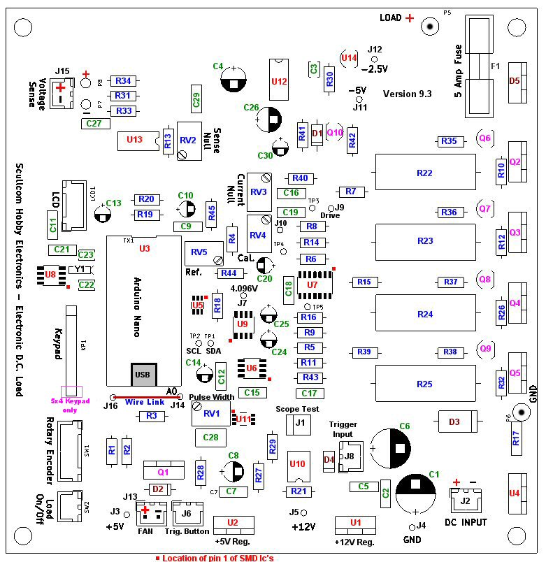
The PCB (version 9.3) gerber files can be downloaded from the link below:
http://www.scullcom.com/DC_Load_ver9_3_gerber_files.zip
The version 9.3 schematic, component layout and updated parts list can be downloaded from the link below:
http://www.scullcom.com/DC_Load_ver9_3_files.zip
Great projects and thanks for your work!
I cannot compile the Electronic DC Load software. Where can I obtain the LCD.h library ?
Phil
https://bitbucket.org/fmalpartida/new-liquidcrystal/downloads/NewliquidCrystal_1.3.4.zip
Hy,
Can you attach the KICAD Layout and schematic files?
I would like to modify it for SMD resistors and capacitors, also to increase the track width for MOSFET.
Hi,
The latest version of the DC Load PCB is now version 9.3. – I made a few improvements.
I have made the KiCad files available for download, link below:
http://www.scullcom.com/DC_Load_Ver9_3_KiCad_Files.zip
Regards,
Louis
Louis
Are there any boards left?
Got any boards left? I posted on Youtube but found your msg on Vid 9. I would like two boards and if possible the double sided ones.
Thanks,
Nicholas
Hi Nicholas,
I have sent you an email with details.
Best regards,
Louis
Hello Louis, Do you have any boards left? – I have been looking at this project since you started it, but have never liked the idea of making my own PCB. Also, do you have a BOM for the project? I may have missed it along the way…
Many thanks,
Ken
Hi Ken,
I have just sent you 2 emails with regards your inquiry. I have just received a few new PCBs which now uses 2oz copper. If you would like one.
I also sent you the files of BOM and other info for version 9.3 PCB. But below is also a link to a zip file with that info as well as it may be of interest to others to.
http://www.scullcom.com/DC_Load_ver9_3_files.zip
Best regards,
Louis
Just got the boards. Thank you so much for sending.
Nicholas
HI Nicholas,
glad to hear they arrived OK. Thanks.
Louis
Hello Louis.
Thank you for great and elaborate piece of work.
Would be still possible to obtain one or two PCB if you had some on stock?
Regards
Kris, Italy
Having similar problem….
ttps://bitbucket.org/fmalpartida/new-liquidcrystal/downloads/NewliquidCrystal_1.3.4.zip
Is not available
I have watched almost all of your videos. Can I suggest an upcoming project? I would like you to design/build a >=200MHz Frequency Counter that can also measure down in the Tens of Hz range. Perhaps it would be useful to have the Frequency Standard/Reference be used to test or calibrate the Frequency Counter…?
Thanks for your comments. I will have a look at the possibility of a project on a >=200MHz Frequency Counter when I have a little more time.
Hello,
much very nice project, brillant video from start to end! Personally prepare on Milliohm-Meter + this Electronic DC Load. Could it be speed Frequency Counter with 10 ÷ 12-digit. 8-digit them on flabby is much, only choose… Great job!
I am sorry for my English.
Regards, Roman Klíma (Czech Rep.)
Thanks Roman.
Hey Louis
Is there any chance you will publish the PCB CAD files?
Thanks
Nick.
P.S. I have made the Millivolt metre using the OSHPARK PCB and added a soft power on.
Keep up the great work.
Hi Nick,
As the project is not fully finalised the PCB keeps changing I have not completed a new PCB yet.
However, one of my followers Rob Bruno has already designed a new PCB using my design (up to Part 5) but we have not tested it yet. It should be OK and uses surface mount components. If you are interested it is available from: https://www.oshpark.com/shared_projects/tXUxCSVa
The PCB CAD file I think is also available to download from OSHPARK.
You can also download the circuit from the link below:
https://www.dropbox.com/s/orwivgbt23gl158/ElectronicDCLoad1.pdf?dl=0
We will be working on a final PCB design which will incorporate all the changes/additions.
Regards,
Louis
Thank you
Hey Louis,
This is a nice project, and explained up into all details! 👍
I have a question that i did not want to ask on your youtube channel,
because it is a bit out of topic :
Do you think i could use such a DC electronic load with AC low voltages,
by connecting it through a bridge rectifier ?
It would then emulate an AC resistive load… ( i suppose ? )
What could go wrong ?
Best regards and thank you for all your nice projects!
Eddy.
Hi Eddy,
Adding a bridge rectifier could allow you to use it on AC. I do not think anything would go wrong.
Give it a try.
Regards,
Louis
Hello Louis,
Thank you very much for your video’s on youtube, as I said on one of them they are Brilliant and the best I ever scene. I have learned so much from you. As soon as I found out you had a website, i had to come here. I had a good feeling from the first time I watched your videos, I knew, you would have had to be a teacher at school as well, especially the way you were waving the stick at the board… lol. No really its because of how you conduct yourself with the expertise of explaining the theories and a perfect tone of voice and temperament. I have to say the tone of voice is very important for teaching, because if it is irritating it is very hard to concentrate after a while. Not to put him down, for example Dave Jones is excellent with his videos and is very talented, but I cannot listen for too long because his voice has too much accent up and down tones and so on.
So I thank you for your work, I think you are a great teacher and kind hearted, I wish I would have had teachers like you!
Now regarding this DC load , it looks like that for now it’s still open to new changes, what do you think about the idea of making the system outputting the data values to a pc and then may be with an already made freeware software it can be data logged to give a record of the load test?
Also I noticed that you made a function to zero the figures at the start by pressing and holding two buttons.
I am just going to ask here so excuse my ignorance, why not have this to zero by its self in the program after turn on and a set delay or every time the load is turned off ? In the past I have made some projects to do this.
Kind Regards,
joe
I have think like you.
Now I’m working about electronics and electrical it very hard to understanding for me.
But I must make Electronic load for ending project.Then in around 2 months ago,I had see this project on youtube but I not good for English I’m Thai and I follows the video.
For now I think I can do that to 30% I had installed for test on breadbroad.
But I had something different to used.
My devices are different from Scullcom project list.
– x2 MCP3425 for ADC devices (now it’s make me a problem because it have the same registor).
– IRF2807 for MOSFET.
– 1ohm tolerrent 5% 7watt for current sence.
– another resistor is tolerrent 5% 1/4watt.
– x2 LM358 for op-amp.
– BC337 for NPN to fan 12v.
please if you have a time I need to known more Louis
Thank you & Best regard
Tae
Hi Louis,
When I wrote the above comments I was just writing my true honesty with out thinking too much on how they may effect another person. So If you think some of my comments about another individual may be offensive as I realized they may be taken that way even though none are intentional. You may remove my letter or if you allow me I would like to comment out that part.
kind regards,
joe
Hi Joe,
Sorry for the long delay only just seen your message.
I would not worry, I do not think anyone will take offense.
Regards,
Louis
Hello,
its great job , i have just one question can i replace mosfet by BJT for exemple TIP 142 ??
Dear Luis. My name is Niki. I’m 37 years old. I’m an engineer and I’d like to improve your existing PCB design for the DC load project you have made.
I have tried to find your email but unfortunately, I can’t.
Please give me your contacts. I have designed already some files. You can see them here:
https://ufile.io/3mot6
and the current (not ready yet PCB design)
https://s2.postimg.org/t5g4vi2kp/pcb1.png
https://s2.postimg.org/z7nrlzr0p/pcb2.png
Thank. Waiting for your answer.
Niki
Hi Niki,
Your links do not work.
Regards,
Louis
Very good projects: thanks.
Perhaps you could consider adding a master list somewhere of all your projects, or even just the main ones.
Adding the latest links to PCB, software etc on that.
As well as your Youtube video links.
And even any related links from your followers.
And a rough summary of the overall specifications of the project.
They don’t need to be accurate during the project, but it is nice to get a rough idea of what a given project can do without going thru the videos in detail.
I tend to get a bit lost in following the various Youtube projects because they do change a bit over time as you modify things.
And an idea for a video might be for you to describe some useful tools that a apprentice electronics hobbyist should consider having, to be a generalist.
Thanks again.
i love your projects thank you so much i have learned so much from them! I would ask if you ever find the time if you could maybe do a video going over the software from top to bottom, similar to how you did with millivolt meter part 2, i have watched that video a hundred times and it makes more and more sense each time! although i would like to see explained a program which controlls a DAC because i cant for the life of me figure out how to use my DACs i have for this load, its a ltc1448 dual channel spi/ 3 wires but to control it it doesnt have any control bits etc, just send a 24 bit word, 24 clock pulses etc, 12 bits go to dac a and 12 to dac b, it makes no sense to me how to ! but just having a explanation of your software would help so much! thanks so much for your time and keep making great videos!
Hi Louis,
I was planning from some time to make an electronic load, and collected the documentation of several projects in order to not reinvent the wheel. One of my goals was to be able to control it from a PC in adition to be a stand alone unit, so the instrument should have a microcontroller, an Arduino if possible, with the software sources available.
Now that I have found your project, I will built it since it seems to me that you have addressed all issues in the analog part so I could center my efforts in adding some capabilities to the Arduino program.
Since I have designed and built several PC controlled instruments that also uses Arduinos at the other end, I already have most of the building blocks (protocols, virtual instrument layouts, logging, graphics, calibration, etc.) for implementing added functionality in an easy way.
I found a guy in Germany who sells PCBs for this proyect and I have bought his last unit. Now I have to order the materials and when the unit is built I’ll begin to add things to the Arduino code. I will keep you informed of the progress.
Thank you for making your projects available.
Hi Ignacio,
Sorry for the delay but have just seen your comments.
I have just designed a new double side PCB which I am making available for purchase. I have already sold some on eBay and should have a new batch of PCB’s soon.
Best regards,
Louis
I would like to purchase double sided pcb when you have them available
John
Hi John,
Just got a new batch in today. Will hold one back for you. Sent you an email.
Regards,
Louis
Hello Louis,
I saw your youtube video’s and think it’s a very nice dc load. I would like to build one but sadly the ebay site says your unable to accept payment and wil not finish the purchase.
Please advise
Hi Kampe,
I will send you an email so I can help.
Regards,
Louis
Hi Louis My name is Christer and i wonder if you still sell some pcb to this projekt
Hi Ignacio
I would be delighted to hear more about your side project for the DC Load.
A PC data logger could come in handy.
Regards
Flemming Loua Christiansen
Hello. First congratulations on these videos. You share an enormous amount of knowledge with them.
I’m am starting electronics, has a hobby, self learning, no knowledge on the area.
I got a little place to have a small lab, and I am looking for DIY tools. So every lab should have a DC Load and your is great work.
I saw almost all your videos and I signed up for the channel. I intend to build some of your projects.
Looking at the last video from the DC Load series I see you have a new PCB.
My question is, will you share the Kicad ou gerber files for this last revision?
Thank you very much.
Forgot to ask, what will the cost of building this you think it is? Approximately of course.
Again, thank you.
Hi Helder,
The total cost is approx. £80 but that assumes you may already have some of the small components already available. I have not calculated a full cost so far if you have to buy everything. Also the cost of components varies a lot depending where you buy them.
Regards,
Louis
Hi Helder,
I will be making my KiCad files available later. At the moment I have been having some PCB’s made which I am offering.
Regards,
Louis
Hi Louis,
I been following your series on the DC Load project and very impressed with it’s evolution. As I intend to build one (probably sooner rather than later now) I would be interested a one of the PCBs that you may have available as stated on the Youtube video.
Best regards,
Richard
There are no PCB’s on the provided link… Since there was pcb files on version 7 of the files, that’s why I was asking if there will be on this version 9…
Hi Richard,
I have just sent you an email and will reserve a PCB for you. To my surprise the first batch on eBay sold in a day. I have a new batch due by the end of this week and reserve one for you. Please reply to the email I have sent you.
Best regards,
Louis
Hello
Can you reserve me a PCB for your super project Build DC Load
cordially
Gérard Daprey
Hi Gérard ,
I also saw your message in You Tube and have sent you an email. I will reserve a PCB for you.
Regards,
Louis
Hi Louis,
Please would you let me know when the new PCBs are available on ebay as I also wish to buy one. Better still, if you could reserve one for me I’d be very grateful.
Regards,
Kieron
Hi Kieron,
Just got a new batch in today. Will hold one back for you. Sent you an email.
Regards,
Louis
Louis, when do you expect the next batch of PCBs to be available? Will you please post a short update video when they are because I would love to order one.
Also, would you consider posting links to shopping carts from the major suppliers that contain all (or most) of what you need to purchase to complete the project? If so I would consider putting together one for the US market if you would post it in your video notes. I can compile it from your notes in the last video and send you a link if you would post it.
Hello Louis,
thank you for your great youtube channel and posting your Electronic DC load project — it looks very well done and I have an itch to build up one.
Can I get one of the DC load PCBs, too?
Regards,
Christian
Hi Christian,
Sorry, just seen this message. But you have a DC Load PCB on its way to you.
Regards,
Louis
Louis
Do you have plans to get any more pcbs (for the DC load), they seem to be disappearing like the proverbial hot cakes!
Thanks
Peter
Hi Peter,
Just got a new batch in today. Will hold one back for you. Sent you an email.
Regards,
Louis
Ohhh – so there is a forum! So I thought I had everything in place, but C6 exploded on me – or at least it looked like a short. I had normal voltage (5 and 12v) before I inserted that cap – I used a 16V cap which I guess may be the issue here. Suggestions? I’ve ordered a 25V 220uF cap but it will be a while before it’s here. I have plenty of 16V but yeah – BOOM! 🙂
Hi,
Do you still have the PCB for the DC load and if so how much are they?
I couldn’t find them on eBay.
Regards,
John
Hi John,
Just got a new batch in today. Will hold one back for you. Sent you an email.
Regards,
Louis
Hi Louis, I’ve certainly enjoyed your series on designing and building the Electronic DC Load.
Your an excellent teacher and imagine yo7 to be thorough and patient.
I see you PCBs available for the project. Is there anything in particular 8 need to do to buy one from you? I’m in Australia.
Hi Michael,
I have no problems sending PCB’s to Australia as I have already sent 4 there so far with out any problems. If you use the eBay link below you can buy from there:
https://www.ebay.co.uk/itm/292490055657
Any problems let me know.
Regards,
Louis
Hi again Louis,
I noticed that the link in Part 7, to the Kicad Files.zip is broken and takes one to the YouTube video for part 7 or some of the Arduino code. Could I ask you to fix it please
You wouldn’t happen to have your parts list available as a spreadsheet would you. If not I’ll prepare one for placing a parts order myself.
Thanks,
Mike Vogel
Hi Michael,
I will have a look at why the link on Part 7 is broken. The KiCad files are the older version.
I will see if I have a spreadsheet as I know some of my followers have made one. If I find it I will email it to you.
Regards,
Louis
Hi Louis,
Thanks for your work on this project. I’m looking forward to building one myself. I checked the ebay link for a pcb but it appears the listing has ended.
Alternatively, would you mind sharing the kicad or gerber files for version 9? Thanks again!
-Phelps
Hi Phelps,
I tried to email you but your email address does not work.
Regards,
Louis
Hi Louis, sending this message with another email address. Hopefully this works.
Hi Phelps,
Have sent you an email. This one has worked this time.
Regards,
Louis
Awesome work on this electronic load Louis!
I too was wondering if I can get the PCB files for that latest version? Or do you have any spares you would sell?
Thanks!
Ken
Hi Ken,
I have sent you an email. I have a few spare PCB’s left.
Regards,
Louis
Hi Louis,
awesome project! I already built the Millivolt Meter and the Milliohm Meter, and both projects are really outstanding. I love your videos, being an amateur myself, they are great learning resources!
I would really like to build this one as well. You don’t happen to have any PCBs left, do you? Ebay is down to zero…
Best regards, and keep up the good work!
Rudolf
Hi Rudolf,
I have sent you an email with details as I still have a couple PCB’s left.
Regards,
Louis
Hi Louis.
As discussed via eBay. I was wondering if there’s still a PCB left.
Kind regards,
Klaas-Jan.
Hi Klass-Jan,
I have a spare DC Load PCB. I have now sent you an email which you can reply to with your delivery mail address.
Payment can be made via PayPal as explained in my email to you.
Regards,
Louis
Hi Louis,
I have watched many of the projects you created but had a problem subscribing to your channel , I am now. I am very interested in building the latest version of your dc load with the new pcb and keypad, I went to buy the pcb at the link provided but the listing had ended.
Is it possible for you to produce one for me, I have a paypal account so could send the money to your email or if you have a different prefered method. I have ordered a lot of the components from ebay and they should come in a few weeks. please keep producing these wonderful projects your channel is my favorite because of your teaching methods, and also the projects being test equipment which the hobbyist could never afford to buy. if I may suggest a proggramable psu would be a great following project.
Regards John.
Hi John,
I have sent you an email with regards your request for a DC Load PCB.
Regards,
Louis
Are you planning an additional manufacturing run of PCB’s.
I missed the last Ebay listing.
I also asked the same question on the You tube posting.
Are there any plans to have a data out capability for logging the results on a PC or similar?
Many thanks for your super detailed contributions to the Electronics Hobbyist community.
Hi David,
I have just ordered another batch of DC Load PCB’s and should have them in about 6 days time. I will send you an email with details.
I do have an idea for data logging using the serial data output to a PC.
Regards,
Louis
Hi Scullcom, I am chasing the PCB for this design. as per your recent communiqué, I have listed my email below.
Looks like I may have posted this in the wrong project
Hi Bruce,
I will now send you a private email to arrange PCB.
Regards,
Louis
Hello,
really great project. I want to order PCB but was already gone :(. Is there another batch of PCBs on the way?
BR Sandi
Hi Sandi,
I have a new batch of PCB’s arriving in the next 2 days. I will send you an email so we can arrange one for you.
Regards,
Louis
hi Louis, I want to order PCB, please send me an email if possible. thank You. Vincent-
Hi Vincent,
I have just sent you an email. I have just had a new batch of PCB’s delivered today.
Regards,
Louis
Hi Louis! Can you please share the KiCAD PCB files? I’m trying to buy the original PCB via eBay but unfortunatelly it doesn’t ships to Argentina (that is where I live ofcourse). So if you please send me the files I can send the PCB to be fabricated some in China.
Beyond this please let me congratulate you on the excellent projects that you do. I find them very interesting but mainly excellently well explained.
Thanks a lot and best regards. Sorry for my bad english,
Mauro.
Hi Mauro,
I will send you an email and try and helps with regards PCB.
Regards,
Louis
Hi, Have you any pcbs left?
Hi David,
I do have a few PCB’s left. I have sent you an email with details.
Regards,
Louis
Louis,
You have sparked my interest in this project and would like a go at it. When/if the next batch of boards arrives I would like my name on one?..
Thanks
Hi Donn,
I do have a few spare PCB’s left. I have emailed you with details if you would like one.
Regards,
Louis
Hi Louis
This is such a great project! I really enjoyed following you along how you improved it step by step. Now I would like to build one. Do you have a pcb left?
Thanks
Kai
Hi Kia,
I do have a few spare PCB’s left. I have emailed you with details if you would like one.
Regards,
Louis
Is it still possible to get a board to build the dc load project? I am In Canada.
Hi Ghislain,
I do have a few spare PCB’s left. I have emailed you with details if you would like one.
Regards,
Louis
Hi Louis,
I have watched all your 10 videos (within one day !) and I find your DC Load project really outstanding.
Would it be possible to order the PCB, as I would like to build the one ? I am in France.
Regards
Adam
Hi Adam,
I do have a few spare PCB’s left. I have emailed you with details if you would like one.
Regards,
Louis
Hi Louis,
is it possible to get a PCB?
thanks so much!
Chiang
Hi Chiang,
I do have a few spare PCB’s left. I have emailed you with details if you would like one.
Regards,
Louis
I too Have watched many of your video and tehe parts for this project are almost all ordered. I too would Like a PCB of this project. I am based in USA Thank you for everything you do.
Hi Gene,
I still have a few spare PCB’s left. I have emailed you with details if you would like one.
Regards,
Louis
I would like to order 2 pcb’s
Hi Ad,
I do have a few spare PCB’s left. I have emailed you with details if you would like one.
Regards,
Louis
Dear Louis,
I’m interested in getting one of the latest PCB’s for the DC load.
Would you still have one for me ?
Kind regards,
Jurgen
Hi Jurgen,
I do have a few left. I have emailed you with details.
Regards,
Louis
Hi Louis
Maybe a bit late, but I discovered your splendid forum and was wondering if it is still
possible to obtain the latest PCB for the DC Load.
,Bests regards
Patrick
Hi Patrick,
I have sent you an email.
Regards,
Louis
Hello,
To increase the power try these PHP79NQ08LT.
Are you coming? To be safe for this project?
Congratulations on the project.
Greetings Vito
Hi Vito,
Thanks for your comment and for the information on an alternative Power Mosfet. The PHP79NQ08LT looks like a good alternative with improved power handling. It may also be easier to purchase.
Regards,
Louis
Hi Louis!
Just recently dicovered your Youtube channel, great stuff.
Really like the DC Load project and it’s a usefull bit of kit I´d like to build for myself.
Any chance you still have some PCB’s left?
Best wishes from Sweden
Michael
Hi Michael,
I have sent you an email with details. I have just had a few more PCB’s made in which I have added some extra grounding, in addition I have also taken the opportunity to add an extra pin to the keypad header to cater for the 5×4 matrix keypad.
Regards,
Louis
Hello,
Do you have any pcb?
Can you give me some 5×4 keyboard?
Greetings
Hi Vito,
I have sent you an email. I can help with both a DC Load PCB and 5×4 matrix keypad.
Regards,
Louis
Hi.
Great project! I would like to build one myself. Do you have a PCB left (I live in Spain).
Thank you.
Hi Mariete,
I have sent you an email.
Regards,
Louis
Hi Louis,
I’ve been watching your DC electronic load project from the beginning, very nice!
I would like to build one, do you have some PCB’s left with the latest mods?
Best regards, Mauro.
Hi Mauro,
I do have a few new PCB’s with the mods on. I have sent you an email.
Regards,
Louis
Hi Louis,
Thanks for your time and effort producing great content and practical projects. Dissecting your projects has increased my understanding exponentially. I’m looking forward to your next project.
Please let me know when your next batch of PCBs arrive. I’d love to purchase one.
Hi James,
I have sent you an email about your PCB request.
Regards,
Louis
Hi Louis,
I’ve replied to your email (in case it ended up in spam folder)
Hi James,
Yes I received your email from a different email address and replied to it. I have now also sent an email to your other email address with the details. Your DC Load PCB was posted to you Tuesday 29th May.
Regards,
Louis
HI Louis.
The revised PCB (v9.3) looks great. Much better without all the copper wires. Thank you once again contributing to the community. Very educational for me and a great bit of equipment to own at the end.
Cheers Alex from Wollongong Australia
Hello Louis,
I´m watching the DC Load project for a while now and I think your way of explaining things is the best I´ve ever seen on Youtube. Thanks a lot for that.
I would like to get on of those DC LOAD PCB´s if there is one left.
Would that be possible?
Regards
Michael
I’m a bit confused around how the sense is connected. In your last video you show that the sense and the load is “just” connected via the switch. I had the sense input go into the sense plug on the board – if you just connect them directly in the way you show, what goes into the PCB sense plug?
Hi Peter,
I will draw a diagram and email it to you.
Regards,
Louis
Hi everybody.
I’ve worked a while on the DC Load project with great fun.
I ended up writing a new software for the Arduino, mostly to learn how to do it.
If you’re interested, take a look at https://bitbucket.org/Rytikar/dcload/src/master/
Have fun and thanks for a fantastic project
Regards
Rüdiger
Hi Rüdiger,
Thanks for the link to the software and documentation. It looks very impressive and I am sure it will be of interest to others who have built the DC Load.
All the best,
Louis
Any chance you have gotten to the 4×5 keypad version yet?
Hi Louis,
I’m interested in getting one of the latest PCB’s for the DC load in the version 9.2.
Would you still have one for me ?
I´m from Brazil.
Best regards,
Jurgen
Hi Jurgen,
I have sent you an email with details.
Regards,
Louis
Hi Louis,
I’m interested in doing this project and i I would like to optimize it. I want to change all the resistors in SMD and to use another ADCs and optimize the cost for project. Can you send me on email all the files for code, layout and schematic ?
Thanks 🙂
Hi ciprian,
I did provide all the download links in the comments below by YouTube video:
https://www.youtube.com/watch?v=FkvvmR4_D-A&t=23s
Below is also the link to the latest KiCad files for PCB version 9.3 where I made some improvements:
http://www.scullcom.com/DC_Load_Ver9_3_KiCad_Files.zip
Arduino software update for 5×4 matrix keypad option:
http://www.scullcom.com/Electronic_Load_software_V35.ino
Arduino software for 4×4 matrix keypad option:
http://www.scullcom.com/Electronic_Load_software_V35B.ino
The schematic and all other documents are in the zip file below:
http://www.scullcom.com/DC_Load_update_files.zip
http://www.scullcom.com/DC_Load_additional_files.zip
http://www.scullcom.com/DC_Load_ver9_2_gerbers.zip
Regards,
Louis
hi, i cant download anything from your server. maybe the server is down?
try to download
http://www.scullcom.com/DC_Load_ver9_3_gerber_files.zip
the scullcom.uk is up but all the link is for scullcom.com
thanks.
Hi Yuri,
I have just tested the link. It is working OK now.
Regards,
Louis
Hi Louis,
Now the links working OK, maybe there is a problem with my ISP.
first of all you make a great project, thanks for your hard work.
but i want to make some changes to the project, i want to achieve 80V 30A 300W module, what changes should be made to achieve the goal, besides replacing the MOSFETS, is there a need for a software change? changes in electronics?
today is a 4 MOSFETS which can reach up to 12A, Will the measurements in the high currents be accurate?
thanks, Yuri.
Hi Yuri,
This project is not capable of 30A you would need hardware changes and software changes.
Regards,
Louis
What is the maximum current for this DC Load Louis?
Hi Louis,
Thanks for this great project. I’ve stuffed all the parts except the power mosfets on the version 9.2 board. I fired it up to check things were working before proceeding with putting in a box but I got nothing on the display. I ordered a new display in case that was faulty but I get the same result. I believe the programing of the Nano is fine and there are digital signals going to the screen. Do the mosfets need to be in? I wouldn’t think so. What else could I check other than the obvious, components in correct orientation and checking for shorts, all which I have done.
Thanks, Rick
Hi Rick,
I think your problem may be due to the fact that your I2C module on the LCD Display uses a different address.
Look for the following line in the Arduino code:
LiquidCrystal_I2C lcd(0x27,2,1,0,4,5,6,7); //0x27 is the default address of the LCD with I2C bus module
The 0x27 in this line of code is the I2C chip address. This may be different with your LCD Display. Try changing this line of code to read:
LiquidCrystal_I2C lcd(0x3F,2,1,0,4,5,6,7); //0x3F is the default address of the LCD with I2C bus module
This will now use the address 0x3F which is another common option used by some displays with a i2C module.
You can download some additional information I have prepared fro the link below, one of the documents in this files gives you a full explanation of the issues:
http://www.scullcom.com/DC_Load_additional_files.zip
Regards,
Louis
http://www.scullcom.com/DC_Load_additional_files.zip
Hello again Louis, and as I said before, what a great project!
Currently I’m trying to buy the parts to make the project. In the meantime I building a very basic DC load (a multi turn potentiometer, an op amp and 3 MOSFETs in parallel). But currently I’m having 2 problems:
1)_
If I use single supply (+9V), at 0V in (+ input of an LM358) the load current is aprox. 850 mA. It looks very very high for me, is this ok???
If I use dual supply (+9V / -5V), at 0V in the load current is aprox. 25 mA, a lot less! But I can’t understand why when I use single supply the load current is so high (I’ve had already check the VGS voltage but honestly I don’t remeber now what the was the value).
By the way, I’m using 3 IRF3205 in parallel, and as far I know, at 0V in the LM358 output must be “almost 0V” (is not rail to rail, but it can reach “almost” 0V at the output). So, checking the IRF3205 datasheet I see that the lowest threshold VGS is 2V. Then, finally, at 0V in (+ input of LM358) the MOSFETs must be completely open right?
Today I’m going check again the VGS voltage when I’m using single supply and at 0V at the input.
2_
As I said, using dual supply I can lower the load current to 25 mA aprox. Now I’m trying to null it completely, so I had implemented the offset null solution that you have presented in part 7, and guess what, it works like a charm!
The only problem is that I can’t figured it out how it works. Its looks pretty simple but I don’t realise. So, can you please explain how this very basic circuit works?
Thanks a lot and best regards, Mauro.
Hi Mauro,
I have sent you an email so you can send me a copy of the schematic you are using.
Regards,
Louis
Louis, I wonder if you had received my mail?
Update:
I’ve detected that the 3 MOSFETs are wrong! When I replace all of them the DC load drains aprox. 0A at OV input, but currently I’m having a very big problem with oscillations! I’m working on that. I will keep you up to date when I have any news.
Thanks a lot and best regards,
Mauro.
Hi Mauro,
Sorry for the delay. I have just sent you an email with some info.
Regards,
Louis
Hi Louis. I’m assembling the PCB 9.3. I ordered all the parts in the parts list. There is a discrepancy in the parts list and the kicad files. I noticed that the 10uF tantalums did not fit all the footprints, then the kicad files show 100uF.
Oh wait there is note in the schematics ! 🙂
I have the ICL7660. Then I can drop the 10pF (C3) and use 10uF instead of 100uF I suppose on C4 and C26.
Seems like its all there anyway.
Great project btw !
Glad to hear you spotted the info on the schematic.
Regards,
Louis
Louis
Here is Kenneth Lavrsen who also commented on your channel and built an electronic load with yours as a major jump start.
I also make music. 100% amateur – no money involved – just fun – should practice more. I made a song as a small humble tribute and a great thank you for your wonderful channel.
Available at https://www.lavrsen.dk/foswiki/bin/view/Music/Scullcom
If it does not fit your taste or it is inappropriate then let me know and I will rename the song and put another story and image. It is just for fun.
Thanks Kenneth for you music tribute and your kind comments.
Best regards,
Louis
Dear Mr Scully Thanks a lot for your great videos ! You’ve learned me an incredible number of things ! I have a question about the Arduino Nano you use in several projects, like your Electronic load. You inject a regulated 5 volts directly into the 5V pin of the board, without protection diodes or voltage management system. Isn’t there a risk to damage the voltage regulator of the board ? And how to you upgrade the software with the USB cable? Do you first remove the Arduino board from your own PCB ? I wonder how you prevent the risk of conflict between the regulated 5 volts supply and the 5 volts coming from the USB plug ? … Thanks again for your excellent work! Yours, Patrick Bertholet
Hi Patrick,
You can inject +5V in to the +5V pin of the Arduino Nano as long as you do not connect any input voltage to the Vin pin. With no voltage on the Vin pin of the Arduino Nano the 5 voltage regulator on the Arduino Nano is not in circuit so there is not an issue.
You upgrade the software on the Arduino Nano by the USB cable. You can leave the Arduino Nano plugged in to the DC Load PCB. There is an isolating diode already on the Arduino Nano which will isolate the USB +5V input if the Arduino Nano is already receiving +5V from the DC Load +5V supply. In this case the +5V coming from the USB lead is in effect disconnected by the isolating diode on the Arduino Nano. If you have a look at the Ardunio Nano schematic you can see this diode (D1). Here is a link to the schematic:
https://www.arduino.cc/en/uploads/Main/ArduinoNano30Schematic.pdf
Hope this helps,
Regards,
Louis
Hi Louis
Thanks a lot for your kind answer and for the schematic! My Arduino Nano clone is a little different from yours, but it has the same type of diode to manage the onboard 5V and USB power line. And yes, it works !
I have a suggestion for a future video, when you have time… Could you explain us the correct way to measure very small voltages and currents with a multimeter ? I do have a pretty good meter -Fluke 87 V- but i think i don’t know how to get the best of it. And i don’t fully understand how the four-wire measuring technique works…
Best regards,
Patrick
Hi Patrick,
Glad to hear it was helpful.
To read small voltages on your Fluke 87V. After selecting the DC voltage range – press and hold the backlight button down for about 1 second or so, the display will then change to give you 4 decimal places when measuring small voltages.
The Fluke 87V does not have a 4 wire measuring option. This option is normally on a good bench multimeter, this option is normally used for measuring low resistances. Two leads are used to supply a fixed known current through the unknown resistance and the other two leads measure the voltage across the resistance so the resistance can be accurately be calculated, as no current is flowing through the second set of leads used to measure the voltage across the resistance the length and resistance of these leads will have no effect on the voltage read across the unknown resistance and so the meter will accurately calculate the unknown resistance.
Regards,
Louis
Hey Louis
Thanks again for your kind and patient explanations ! I will train myself with your other projects, like the milliohm meter and the precision current source. Recently, i also read (again) your video on PCB making at home, which is great. I still make my PCBs myself, with Kicad, a small insulator and presensitive boards, but i only did single side boards for the moment. Do you plan to make a video on DIY double-side PCBs ? I would be glad to get some tips from an expert !
Yours,
Patrick Bertholet, France
Hi Patrick,
Sorry for the delay but have been away on holiday.
Making double sided PCB’s yourself can be a bit tricky as you need to accurately alien the exposure films on both sides of the PCB. The best way to do this is to have alignment holes in each corner of the film which match for both the top and bottom transparency films – then mark and drill these holes on the double sided copper board and align the films with these holes. the trick bit is ensuring that they stay aligned during exposure to the ultra violet light.
Regards,
Louis
Hi Louis,
I have been enjoying your great videos. Easy to follow. I really would like to put together your DC load project. I was wondering if you still have any PCB available?
Thanks again
regards
Sandy
Hi Sandy,
I have sent you an email.
regards,
Louis
Hey Louis
I have just come across your fantastic project when trying to solve my requirement for a DC load for my project. Do you have any PCBs still available for sale? I am UK based.
Kind Regards
Paul
Hi Paul,
I have just sent you an email regarding the PCB.
Regards,
Louis
Hi, I’ve been following this project on YouTube and I was wondering if you sell this as a kit that can be built? I’d be very interested in buying one. I build a lot of laser drivers and this would be very useful in testing these drivers.
Hi,
Sorry I do not sell any kits for this project. I do have a few PCB’s left though.
Regards,
Louis
I see. Let me take a shot at making the PCB. I had intended to mostly use SMD component since I have quite a few on stock. I’ll share my design once I’ve tested it. Thank you again for making these videos. The content is great but the little sections of theory that you’ve explained are really useful.
All the best with your SMD version of the PCB.
Regards,
Louis
HI! I both two of your boards just about done building the first one what is the bnc used for and how do you use it and could you Email me a sheet on how to set all those vrs
Hi Guy,
I have sent you an email with calibration info sheet.
You can also download it from the link below:
http://www.scullcom.com/DC_Load_calibration_updated2.pdf
Also check out part 8 video of the DC Load project where I go through some of the preset adjustments:
https://www.youtube.com/watch?v=hhzmU6gOzMo&list=PLUMG8JNssPPzbr4LydbTcBrhoPlemu5Dt&index=8
The BNC socket is used as a Trigger Input for one of the options in the transient mode (pulse mode option). Have a look at part 6 video where I explain this function.
https://www.youtube.com/watch?v=9auu8hH4IPM&index=6&list=PLUMG8JNssPPzbr4LydbTcBrhoPlemu5Dt
Regards,
Louis
Hi Louis (:
Thank you for sharing your great projects!
I am building your DC Load, but i have some issues. The software seems to work okay, but i am not getting any voltage reading on the display when I connect a powersupply to the + and – LOAD terminals. What can I do about it?
Regards Rasmus.
Hi Rasmus,
Sorry for the delay in answering due to the fact we have been away on holiday.
With regards your issue. Can you measure the voltages on pins 2, 3 and 6 of U13. Also measure the voltage on pin 8 of U7. Let me know what voltage readings you are getting on these pins.
Did you wire up the Sense Switch?
Regards,
Louis
Hi Louis.
Currently, I’m just wiring the sense wires in parallel to the 5v power supply, because I don’t have a case for this project yet. I hope this is good enough?
In regards of U13;
– pin 2: 94,1 mV
– pin 3: 100,4 mV
– pin 6: 102,7 mV
In regards of U7;
– pin 8: 102,7 mV
Regards,
Rasmus.
Hi Rasmus,
All those voltages should read about 100mV when you have a 5V input on the Load and Sense terminals. So your voltage readings are more or less OK. The voltage sense IC (U13) is configured as a divide by 50 so with 5V Load/Sense the output reading at pin 6 of U13 should be 100mV, your reading of 102.7mV is just slightly higher but you should be able to adjust this by the RV2 preset resistor. Your Voltage sense circuit U13 is working OK.
The output from the buffer stage U7C should also read 100mV in this situation. You are getting 102.7mV at pin 8 of U7 so that’s OK.
The next think to check is if U6 the ADC is working OK:
First check the voltage at both sides of R5 (100 ohm) are the same – in your case it should read 102.7mV at both sides of that resistor. If this is what you read then the voltage been fed to the ADC (U6) is correct.
Now you need to check if U6 (ADC) is working OK – first do a visual check to ensure you have soldered the IC the correct way round on the PCB (there is a possibility you may have soldered it in reverse in which case it is likely you have damaged the IC).
Next check the following:
When you set a current load (say set a load current of 1.000A) and switch the load on with the keypad do you get a current reading on the LCD display?
If you do not get a current reading as well as no voltage reading then the fault is likely to be U6 (as you LCD display is working OK we can assume that the I2C bus is OK).
Let me know what you find. I will also send this info in an email so you can contact me directly by email for any further help.
Regards,
Louis
Hi Louis,
same issue here. I checked all and I found also that voltage is updated only when I power on the DC Load, and then voltage is still. I checked that voltage read at power on, is same as power source, so it seems ADC work only when DC Load is power on. No current reading durig LoadOn. Strange thing is also a quick blinking of the curson under the second digit of current setting (i cannot see this blinking in your videos). All other readings (temperature, encoder, keypad button) are ok and working fine. Also load working fine.
Thanks in advance
Marco
Hi Louis,
I am having similar issues. I have checked all of the voltages as suggested and they all seem correct. I also ran the list devices sketch from the MCP3426 library and got the following output. Could the ADC still be damaged.
Found device at: 0x27
Found device at: 0x57
Found device at: 0x61
Found device at: 0x68
Found device at: 0x6F
BTW these measurements are taken with the 5v power supply on.
Hey Louis,
first, thank you for this great project and all the work you spent for it. I’m also plan to build your project, but with some changes in parts and layout. During studying your files (hope I have the latest ones), I found some small issues in your layout / partslist (v9.3). I’m sure you found them also and always fixed that, but sometimes four eyes see more than two 🙂
For the choosen 32.768 kHz crystal the footprint is with 1.5×5 mm to small to fit your recommended part AB38T from Abracon, especially if you follow the datasheet and want to fix it with rubber glue on the pcb. There is a smaller version from Abracon with same specs named AB15T that will fit (Farnell order code. 1611825).
There seems to be some updates missing in the partslist (9.3): The wirewound resistors R22, R23, R24, R25 still have 0.1 Ohm not 1 Ohm and R43 should have 1M not 270k.
I try to find a dealer with remainders of the BUK956R1-100E but I was not lucky. So I want to replace it by the STB80NF55L-06, but the datasheet confuses me a little bit. There is only a specification of the min Vgs(th) of 1V and the absolute max rating of 16V. Do you have any recommendations for the right dimensioning of the resistors R35-R38 (2k2) and R10,R12,R26,R32 (270k) for me ?
Hi, Louis!
Could to tell please power consumption of the device? I see it’s 15-18VDC, but what amperage?
I’ve got a transformer with two 18VAC @ 0.2A winding and wonder if it’ll be capable to supply enough juice.
Thank you for your time and effort! This load is a true diy BK Precision 8500 killer xD
Regards, Phil.
Hello Louis!
At first thank you for your enthusiasm in electronics especially for this DC load project! I ordered some pcb’s of the version 9.2 and equipped the peripherals with a 4×4 keypad and a standart rotary encoder knob and a 4×20 LCD. After uploading the software version V35B onto the µC I noticed some issues:
1. Changing the set value (I, P, Ohms) on the LCD via the rotary knob is not doable -> no reactions when I turn the Encoder knob. Have you an idea why?
2. Where is the enter key on a 4 x 4 Keypad? Is it the letter ‘D’?
3. After starting up thr programs comes in stuck due to the ‘TempCutOff’ loop. Thus the LCD is changing between ‘CC’ and ‘Overtemperature’ status. How can I prevent that?
Best regards in advance
George
Hello
What a great construction.
Thinking i will make one for my self.
But it seems that the BUK956R1-100e is obsolete and i cant seem to find anyone who still has it in stock.
Can you help me with an replacement type ?
Best regards
Carsten
Hi,
in the release 9.3 zip file there is a guide for alternative MOSFETs:
Note 1:POWER MOSFET ALTERNATIVES TO BUK956R1-100E (Q2, Q3, Q4 and Q5)
PHP79NQ08LT Nexperia
STP80NF55L-06 STMicroelectronics
RFP12N10L Fairchild
STP55NF06LSTMicroelectronics
(In order of preference)
greetings from germany
Hi Louis
Thank you for sharing your great projects! Love it and thanks for the PC Board
I have the same problem with the availability of the BUK956R1-100e. Can you provide an alternative MOSFET number. I buy all the components from Element14 Australia.
Thanks Again
Hi,
in the release 9.3 zip file there is a guide for alternative MOSFETs:
Note 1:POWER MOSFET ALTERNATIVES TO BUK956R1-100E (Q2, Q3, Q4 and Q5)
PHP79NQ08LT Nexperia
STP80NF55L-06 STMicroelectronics
RFP12N10L Fairchild
STP55NF06LSTMicroelectronics
(In order of preference)
greetings from germany
Great!
PS. If I need no more than 1A load, shall I replace 0.1ohm with 0.5 ohm (for more precise measurement). All voltages will be recalculated.
Dick
Hi Dick,
Sorry for the long delay in answering.
If you change the 0.1 ohm to a 0.5 ohm then you would also need to make some changes to the Adrunio code to take account of this change as your current sense voltage would now be 5 times greater than before.
Maybe a better option is to use a 0.4 ohm sense resistor (you may have to make this using 4 of 0.1 ohm 1 watt resistors – they would not need to be on a heatsink) as this will make it easier to alter the software. This will give you a sense voltage now 4 times higher.
Now look at the Arduino code and find the following lines of code under the —-Read Voltage and Current—- section of the code:
// Initiate a conversion; convertAndRead() will wait until it can be read
adc.convertAndRead(MCP342x::channel2, MCP342x::oneShot,
MCP342x::resolution16, MCP342x::gain4, //”gain4″ means we have select the input amp of the ADC to x4
1000000, current, status);
You will see the gain of the ADC used to monitor the sense current voltage is set for a gain of 4. You can set this to a gain of one and it should work. Change the gain4 to read gain1 in the following line of code as follows:
MCP342x::resolution16, MCP342x::gain1, //”gain1″ means we have select the input amp of the ADC to x1
Hope this helps.
Best regards,
Louis
Hello!
Really like this project. Is there by any chance any PCB:s left to buy?
Vidar
You can get them from: https://jlcpcb.com/quote
Current price is: $15.78 for 5 boards including shipping.
Hi Vidar,
Sorry of the long delay in answering. I have sent you an email with details.
Best regards,
Louis
Louis,
Thanks for a great project.
Please can you put on line the art work for the v9.3 5×4 keypad front panel (to be stuck onto project box.
Thank you.
Peter Fielden-Weston
Hi Peter,
Sorry for the long delay. Below is a link to a direct download the 5×4 keypad stick on overlay.
http://www.scullcom.com/DC_Load_5x4_keypad_stick_on.zip
It was also available for download as a download in my Part 8 video where I gave a download link called DC_Load_9_2_files_zip which included lots of documents and artwork for this project including the 5×4 keypad stick on artwork.
Direct link to that is:
http://www.scullcom.com/DC_Load_9_2_files.zip
Best regards,
Louis
Hi Louis
This is a great project that I want to build. Can you tell me how I can obtain the latest pcb please.
Regards,
Reg.
Hi Louis,
I’m interested in getting one of the latest PCB’s for the DC load in the version 9.3.
Would you still have one for me ?
Best regards,
Hartmut
Hi Hartmut,
I have sent you an email with details.
Best regards,
Louis
Hello
The void BatteryCapacity (void) function is declared twice in your program.
No compilation error
Is this a mistake you a trick I do not know.
Thank you for informing me.
Very nice job
cordially
Gerard Daprey
Hello Louis
I realized your project works perfectly.
First, I specify that I used your version 9.2 double-sided PCB.
The editing worked the first time with an Arduino Nano.
I then replaced the Arduino module with the Mega 250 version which I had already mentioned the existence.
the link :
https://fr.aliexpress.com/item/Mega-2560-PRO-Embed-CH340G-ATmega2560-16AU-with-male-pinheaders-Compatible-for-Arduino-Mega-2560/32801785024.html?spm=a2g0s. 9042311.0.0.27426c37OmZKMn
This very compact model (38x55mm) has been set up with a home adapter in a vertical position, in the original Nano bracket.
No change for the original PCB.
Only a few port values have to change in the code.
You change from 32 to 256 KB of Flash memory and the EEPROM from 1 to 4 KB
So you can upgrade the code without memory limitation and keeping the work done by Louis Scully.
This small adapter can be used for other Nano-based projects.
For those who are interested, I can send the diagram and photos of the adapter by email.
gdaprey at bateau.net
Thank you again Louis for this project
Hi ,
Thanks for the great project, enjoy your video a lot. Wondering if you have boards left , double sided ?
Thanks, Eddi
Hi Eddi,
Sorry I currently do not have any. However, I will get a few more made and let you know when I have them.
Best regards,
Louis
Hi Louis,
I’m interested in getting one of the latest PCB’s for the DC load in the version 9.3.
Would you still have one for me ?
Best regards,
Adrian David
Hi Louis,
First of all, Great Project!!!, I have built it using one of the V9.3 boards off Ebay, but have questions.
All works OK as is but I have tried upping the current limits to 8A for battery testing.
This works up to 4A OK, but if I set 5A the current drops back to less than 1A, is this a design feature or a bug.
I would like to test cells at a higher rate if possible, I have altered the source resistors to be 0.5ohms and adjusted
the protection resistors (270k) to 180k.
I have also noticed the rotary encoder sometimes skips values, would it not be better to use one of the rotary libraries out there that incorporate “keybounce”.
Thanks again for a great project!!
Trevor.
I also have this problem. I designed my own PCB to go up to 10A and once I go past 4, it cuts back to 0.8A and won’t go any higher.
Hi Louis,
Thank you for this project. I have been searching for a nicely designed and feature-rich electronic load and your project fits the bill perfectly. Thank you so much for sharing!
I’d be interested in purchasing one of your PCBs. Please let me know when they become available again.
Regards,
Milan.
Hi Louis
Great project. Would it be still possible to obtain one or two PCB do you have some still in stock ? (Preferably with all components 😉 )
Regards
Dariusz
Hi Louis,
First of all, Amazing Project!!!, I want to build one using your files as a reference, but I can’t download it for some reason that I don’t know, always have problems, is there another way to download it? I’ll apreciate your help a lot,
best regards.
Hi. I want to modify your code to use DS3231 as the RTC chip instead of the MCP79410. But I cannot understand how I will replace the RTC code lines. Can you give me a reference to the statements of the MCP79410 library? Since you made it, maybe you can write an article about the library.
Please reply.
Thank you.
Prithul.
Thank you Louis for this project – you are a very helpful person and people are greatful as they find an interest in electronics and you aid them without payment of any kind – suggestion – possibly put a donation link on your site to fund your projects or for charity as I for one would donate.
I would be interested in increasing the load caperbilities of this project to say 8-10Amps (away from the linit of 4) as mentioned by a few people above.
anyway all the best
thank you again
Stephen
Louis,
V9.3 of the schematic (PDF) seem to have incorrect values fort some of the parts; for example R10, R12, R26, R32 all show 270K, but you mention they are 47K (as also shown in the parts list).
Same applies to R22/R23/R24&R25, which should be 0.1 (or 0.47), but schematic states 1R.
Or am I looking to the wrong version of the schematic?
Hello…Richard here…rfsx15@gmail.com
I recently found your youtube channel and have enjoyed very much the electronic load videos, discussion, and documentation. I would be interested in circuit boards if they are still available.
Thanx for the great project!
I see that you linked to kwong. I am interested in higher power load capacity, ie 60a @ 60 volts. There are a number if IGBT mosfet blocks available of high power rating. Plus kwong uses current shunts. Is this something that could be integrated into your desigh?
Regards…Richard
Thx 4 sharing this Project!
I rebuild your Project (made with IBF-TARGET3001), but it’s still Beta-State.
The dimension of the PCB is 100 * 75mm, double-Layer, and can operate with logic-Level or MosFets/IGBTs, Fet-driver is included.
https://filehorst.de/folder.php?key=cCmIcJ2M
Hello FMMECH_24.
Looks interesting. Is your project in finished state yet? Do you have some reference blog to it with more info?
Regards Kris
Hello Louis,
I love this project and it looks like the best one out there!
I tried to make my own version that could handle more current but I’m having some troubles with calibrating my load. All of the other parts work correctly but the -2.5v and 4.096 doesn’t stay constant and changes when I adjust the current null calibration. There are also other problems with calibration and I’m having an extremely hard time figuring out what’s wrong.
Would you mind sending me an email so that I could share my design with you so that you could take a look and help me figure out what’s wrong?
Thanks so much, keep up the great work!
Hi John,
I make my own version with kicad based on Loius one and use large ground plane on the bottom side. During the first test I recognize this was not enough for a stable ref voltage. So, as Loius recommended, I must also enhanced my grounding by adding some 1.5mm² copper wires. You can try to measure the voltage drop between a ground pin of the supply voltage (U2/U1) and Pin 4 (GND) of the REF5040.
Hello Louis,
I have noticed something in the code “Battery Capacity Discharge Function routine”, that should be corrected, if I am right, this will help improve some speed by changing the Comparison operator on one of your lines.
Please email me direct so I can be more specific, Also I can share a schematic of the final stage of a DC load I have build and tested. its not fully finished!, but can handle up to 350 and 400 Watts.
Kind Regards,
joe
Louis,
I only have one suggestion for the Electronic DC Load.
The printed circuit board should be a 3 layer board or ever possible 4 layer.
Layer 1 – Should the SMD (surface mounted devices) components side and THT (Through Hole Terminal) components.
Layer 2 – The positive layer.
Layer 3 – The negative layer.
Layer 4 – The ground layer.
They can arrange in any order Layer 2,3 or 4 depending on which way the noise induction can be eliminate.
The board will become too expansive to manufacture for home hobbyist. The via with even more expansive between layers.
Kind Regards
Loizos
Electronic dc load it is great to see this kind of work. I am interestedon on buy the project for my personal use. Now you have my email address please let me know what is it that you require to sell the full project. Thank you and I am Looking forward to your answer
Are there any boards left?
wish you had more subscribers! You do top job of teaching hope you put out some more you tube videos. have you thought of patreon
Hello Louis,
I hope you can help me,
I built your dummy load to the following spec 9.3, with php79nq0blt for q3-6.
I cant get the board to draw any current from the load and regardless of the position of r3 and rv4 i get 0A on the lcd for actual current draw
everything else seems to work:
Voltage sense works and is accurate
temperature sense works, fan works,
menus work, rotary encoder works, lcd works, software works, 4×5 keyboard works
I have checked all the voltage test points and they are accurate to within 1%, the fuse is infact.
I have checked the diodes are in the correct way round and all compontnts are the correct values. I have also continuity tested most of the board.
I also checked all resistors and caps before soldering into the board.
the 4096V test point has been adjusted to 4096V without issues and is stable
no componets get excessively hot and the coltage test points are all stable.
I have not tested the trigger side but made the adjustments to rv1 as per your calibarion guide
If I adjust the current draw in the CC screen I note that the voltage opn the drive pin J9 increases until I get past 4A where it suddenly decreases.
ajusting Rv4 effects the drive voltage and the maximum drive voltage for a requested current draw of
1A is 0.1085V
2A is 0.2160V
3A is 0.3238V
4A is 0.4308V
5V is 0.0892V <— which obviously does not follow the trend
The mostfet drive test point is constant at 4.9098V regardless of the set current draw
As accurately as i can measure there is no current being drawn from the load under test under any circumstamces
thank you for your time
regards
James King
Good day,
I am responding to the query of James King. I also struggled with the the 4 Amps max restriction (Trevor Henshaw and John Hofmeyer also mentioned this earlier on). Here is my 5 cents on this phenonema.
The MCP4725 is a 12 Bit DAC and hence has a resolution of 4096 (from 0 to 4095) steps. In the code, each step is set to the equivalent of 100 mVolts. Thus, the maximum steps are reached if the current (=controlvoltage in the code) is set in the LCD menu to 4.095 Amps (or 4,095 Volts of control voltage). Any current (controlvoltage) setting above this value leads to an “overflow” of the DAC counter and at 4095 +1 step, the counter starts to count again from 0 upwards. This is why your reading at 5 Amps is roughly 0,09 Volts at J9 and 0.9 Volts at TP3.
Remember, the DAC can output a voltage between 0 and the supply voltage of the DAC (which is the 4,096 volts). This voltage is then reduced by 1:10 by the R6 and R14 voltage divider. You can change the values of these resistors so that your J9 Voltage is say 0,5 volts at TP3 of say 0,4905 volts. This way, your output Amps will go higher than 4.095 Amps.
Your 2nd problem seams to be a Mosfet related one. the OpAmp is providing the maximum output voltage (5V rail voltage) and still your MosFet is not switching. Are you using a logic level MosFET with a low threshold Gate to Source voltage? If you are using the 1 Ohm resistor at the source, you will have a voltage drop over this resistor, which increases you source voltage. That could lead to a insufficient GS voltage drop and the MosFET is probably not in the “On” resistance range at this GS voltage.
All of what I am saying might be completely wrong, since I know nothing about coding or electronics. Just thinking.
By the way, I really love this Youtube channel and hope Louis Scully is doing well. Has been quite here for a while.
Thomas
Hello All,
After taking Thomas’s advice into consideration I have been able to semi-fix the problem. I am now able to draw up to 7A before my psu cuts out, but I think it should be able to go upto 12A. In order to achieve this, I first changed the value of R6 to 2.4K. This results in a max output voltage of 1.2v when the ADC outputs 4.095v. The next thing I did was change the following lines of code:
void dacControlVoltage (void) {
if (Mode == “CC”){
setCurrent = reading*350; //set current is equal to input value in Amps
setReading = setCurrent; //show the set current reading being used
setControlCurrent = setCurrent * setCurrentCalibrationFactor;
controlVoltage = setControlCurrent;
}
if (Mode == “CP”){
setPower = reading*350; //in Watts
setReading = setPower;
setCurrent = setPower/ActualVoltage;
setControlCurrent = setCurrent * setCurrentCalibrationFactor;
controlVoltage = setControlCurrent; //
}
PLEASE NOTE: While these changes allow me to pull more current I still have the problem that the LCD won’t display higher than 5A. This means that even if I set the current to 8A, the load will draw 8A but it will only display 5A. If anyone knows’s a fix to this please post it.
Thanks, and good luck!
John Hofmeyr
Good day
you can introduce factors in the code to adjust both, the voltage per step for the DAC (output to drive the MosFet) and for the ADC (input which is the reading) to adjust to the desired limits of operation. This comes at the cost of accuracy.
You other option is to reduce the gain of the ADC to 2 (from top of my head, I believe it is set 4 in the code). This was explained by Scully in one of the early videos- when he change from a voltage devider to utilizing the gain of the ADC. He designed the DC Load for a max load of 5 Amps.
Hope this helps. Pls check the max allowed input voltage of the ADC according to the data sheet. I do not have access to it right now. But I think it should be fine so that no hardware change on the read side is needed. Isn‘t it fun to learn this way?
Good day Thomas
I have thought a little more and here is my conclusion:
First of all, be aware that the design was done for a maximum of 5 amps initially.
A calibration factor in the software will not help at all. You will have to reduce the gain factor of the ADC in the software. And you will have to reduce the input voltage at pin 1 of the DAC with an additional voltage divider at the output of the OpAmp. Watch video #3 for more information.
The current measurement is based on the voltage drop over R17. Each ampere of load will lead to a voltage drop of 1/10 of a volt at this resistor.
The MPC3426 is a 16bit analog to digital converter. This means it has a resolution of 2^16 steps which is 65536 steps (-32768 to +32767). It also has an internal voltage reference of +-2.048 volts. Thus, one step is 2*2.048/65536=0.0000625volts per step. Only the positive voltage range of the ADC reference is used, since pin 2 of the ADC is set to ground.
The gain factor, which is a multiplier of the input voltage, is set to 4.
With a load of 5 amps, we get a voltage drop of 0.5volts at R17. The ADC will “read” 0,5*4=2volts. Very close to the maximum of the 2.048volts internal reference. With 0.512 volt at pin 1 of the ADC, the maximum steps of 32767 is reached. Ergo, an increase of the voltage at pin 1 to anything over 0.512 volts will not lead to a higher number of steps. There is a“reading cutoff“ at this voltage, which is the equivalent of 5.12 amps.
To overcome this, just reduce the gain from 4 to 2. In this case, the maximum load reading increases to 10.24 amps.
In addition, the maximum input voltage at pin 2 shall not exceed vDD volts.
Since vDD in our case is +5V, you will have to add an additional voltage divider to reduce the voltage by the factor of 2 (two resistors with the same value – say between 1k to 10K).
Having done this, you increased the max current reading capability of the load to about 10 amps.
You will now get the correct reading, however, the resolution or accuracy of your „“ampere-meter“ is reduced. I guess this should not be an issue though. Just be aware of it.
Finally, set the “setCurrentCalibrationFactor” in the software to 10000/4096 to adjust on the DAC control side for this range and also adjust the voltage divider R6, R14 for the required range (voltage on J9 to go from 0 to 1V max which is the equivalent ot 1V voltage drop at R1,aka 10amps). Now you should have balanced setting – control – reading.
And confirm my conclusion by thinking this trough by yourself. I am still leaning.I usually learn by making mistakes and I have not physically tested this.
Thomas
And you will have to reduce the input voltage at pin 1 of the DAC with an additional voltage divider at the output of the OpAmp….
I meant pin 1 of the ADC of course. Sorry for the confusion.
Thomas
Hello THOMASS,
This is a very nice explanation. As i’m not an expert, there fore I would like to kindly ask your to open a bit on the technical side of it.
“In addition, the maximum input voltage at pin 2 shall not exceed vDD volts.
Since vDD in our case is +5V, you will have to add an additional voltage divider to reduce the voltage by the factor of 2 (two resistors with the same value – say between 1k to 10K).
Having done this, you increased the max current reading capability of the load to about 10 amps.”
This would mean to cut the track the leads to pin 3 (VDD) of the MCP4725, bridge it with 10K and solder extra 10K to any ground correct?
“And you will have to reduce the input voltage at pin 1 of the DAC with an additional voltage divider at the output of the OpAmp….
I meant pin 1 of the ADC of course. Sorry for the confusion.”
What ratio of the devider? How to fisicaly execute this? From where to where to pull it out? I imagine there will be another track cutting from between DAC pin 1 (OUT) to the OPAMP pin 3, more precisely between R4 and PT3?
Thanks in advance
Kris
CORRECTED
Hello THOMASS,
This is a very nice explanation. As i’m not an expert, there fore I would like to kindly ask your to open a bit on the technical side of it.
“In addition, the maximum input voltage at pin 2 shall not exceed vDD volts.
Since vDD in our case is +5V, you will have to add an additional voltage divider to reduce the voltage by the factor of 2 (two resistors with the same value – say between 1k to 10K).
Having done this, you increased the max current reading capability of the load to about 10 amps.”
This would mean to cut the track the leads to pin 3 (VDD) of the MCP4725, bridge it with 10K and solder extra 10K to any ground correct?
“And you will have to reduce the input voltage at pin 1 of the DAC with an additional voltage divider at the output of the OpAmp….
I meant pin 1 of the ADC of course. Sorry for the confusion.”
What ratio of the devider (what voltage as a target?)? How to fisicaly execute this? From where to where to pull it out? I imagine there will be another track cutting from between ADC pin 1 (CH1+) and U7C, more precisely between R43 and C15?
Thank you in advance
Kris
Hello,
I’m having the same problem here with the 4 ampere limit. My DC-load has a gigantic heatsink and I installed 8 driver mosfets good for 8 ampere (there may even be space for more). If someone could make the new software (I can’t do programming…) I’d like to help out testing.
Greetings,
Erik
BEL LAVORO
COME POSSO AQUISTARE I PCB ?
GOOD JOB
HOW CAN I BUY PCB?
eBay – as no one was selling – I have had a few made and have them for sale on eBay for a while with a few left.
https://www.ebay.co.uk/itm/283458246652
I hope this helps
Hello Stephen,
Would you still have a PCB ver. 9.3 available?
Best regards
Hans
You can take the gerber files provided then upload them to sites like JCLPCB and have them made and shipped to you for $50. There is a minimum of 5 boards you must order but still, sell the rest and stop asking him for pcbs, jesus.
Hi, great series, thank you for the wonderful design and enhancement journey, you are a great teacher indeed.
Do you still have any PCB’s for sale?
Patrick
I have done some analysis of the behaviour and measurement caperbilities of the load, and have some observations. Naturally some of these observations depend somewhat on the adjustments for current null and current sensitivity etc but some are calibration independant.
Test conditions: I modified the program so that it displayed the raw values read from the ADC for the current and voltage
I set the voltage adc channel to 18 bit resolution
I set the current adc to 18 bit resoluation and 8x gain
Observations
1. voltage measurement can be made quite accurate.
I shorted the voltage sense + and – together and adjusted the voltage null until the adc outputed 0
I inputed 57 volts and noted the adc output in my case 728001
I then ploted voltages in 10, 5, 1 and 100mv decrements from 57V down to 0 and found the adc to be very linear. I ended up modifying the ActualVoltage calculation to 57.0*voltage/728001. In other words the actual voltage is the voltage read from the adc scaled by the adc output for my 57.0V reference. The result is only around 1mV out over the entire range I could measure 57V-0V. this is very good.
The current side of things is not so good.
2. at low input voltages only small currents can be draw. I suspect this is because of the protection diode on the current input. For example if I want to draw 1A I need about 1V input. inputing only 0.5V means even if I request 1A current draw the device does not draw this much current. Bellow about 320mV no current can be draw regardless of the current draw requested. This makes the device less useful for say nimh battery testing.
3. the current devices measurment is non linear and has multiple issues at around 35mA draw down to 15mA and worse bellow that.
from 2.2A (the most I can draw from my dc supply) down to about 35mA I can get a good fit to the data using a linear function. (2nd order poly is slightly better). Bellow around 35mA the current reading from the dac becomes very non linear and I need to use a completely different 2nd order poly to get anything like accurate results. Bellow about 15mA there is not enough resultion in the dac and all current draws below this valve result in the same output from the current adc. The actual current draw setting produces ok results down to about 5mA. I therefore altered the ActualCurrent calculation to use one curve for adc readings above 1000 (which equate to about 35mA draw) and a different curve bellow that. Accuracy is now good. BUT this does not fix the problem that the protection diode does not allow high current draw at low voltages.
Conclusion
the adc is linear – its the same adc used for voltage and current measurement. BUT so little voltage gets to the adc when measuring current its forced to use internal amplification and this is noisy and not so linear. The result is compromised low current measurement.
The protection diode makes certain combinations of current draw and voltage input impossible.
The dac that controls the current draw is not bad even though its less than 16 bit.
If the voltage adc is not set to 18 bit the results are still linear and predictable but the sub 10mV readings are not so good (lack of resolution). I know the 18 bit setting is using interpolation BUT the dac iss et to 1x gain and so is not running too noisily and 18 bit mode works better than 16 bit in this case
the current dac even if left at x4 and 16 bit mode does not have enough input voltage to handle reading low currents accurately. Setting 18bit and x8 does not help much because its already getting a lots of noise and issues from the gain and this messes up the 18 bit interpolation to.
I strongly suspect that too get good sub 35mA current readings the ouput of the sense resistor will need amplification but a good opamp rather than just being buffered. However this would limit the high current range… So ideally there needs to be a switching mechanism and one op amp gain for currents down to say 50mA and another for sub 50mA currents…
I don’t think our complet comment was posted. Can you forward your complet comment to me? I have built this DC load and I am very interested in your opinions and comments. Thank you and a very large thanks to Louis. mancel@charter.net
Hi Louis,
Congratulations. I was looking for documentation to design my own electonic load with roughly the same features as yours and the same architecture. Your serie gave me a lot of informations and ideas.
My load should be 150V/30A/150W.
I have 2 questions :
– I am using an I²C hall effect sensor instead of sense resistor, why didn’t you use one ? Do you have any feedback on this ?
– Why do you use a schottky to protect the LOAD input and not a TVS ?
Regards
François
Hi Louis,
I just finished the my DC load 9.3 version of your design but while going through the calibration for the amps,
I have run into a problem. At 1, 2, 3 amps inputted into the CC mode, the load draws (passes through) whatever value the dc power supply amperage is set to, turn it up or turn it down, the DC load reads the same as what the power supply reads it is supplying. Before I even started, I went through the calibration on my Kenwood 10 amp 30 volt power supply with a 0 .1 ohm power resistor and my Fluke 87 meter per the Kenwood service manual.
I used the STP80NF55L-06 Mosfet’s bought new from Mouser.
The J9 Drive pin voltage reads correct with the Fluke meter with the amp load requested for the DC load but it does not regulate the amperage.
I checked the voltage drop across the R22, R23, R24, and R25 resistors and they are pretty much the same . When checked with a IR optical meter, two of the power Mosfet’s read the same temp, one of them reads higher, at 4 amps and 30 volts about 30 degrees C hotter and less at lower amps while one reads a bit lower than the two that read the same.
My guess is that the Mosfet that runs hot has a fault and I should change it ( as well as the one that runs colder while I have it back apart).
Do you have any thoughts or tests I could do to check before I tear it apart?
Thank you for the project and thank you for your time.
Mark
Hello Louis. I really like your project.
I want to ask you. Please include subtitles on all videos on your YouTube channel.
I just received a PCB from Steven and it is very good quality. He shipped it out right away. Get one while he still has them in stock.
Now if Louis would get back on the air all would be good in the world.
Hello,
Does anybody have an extra version 9.3 PCB available? I would like to buy one.
Best regards
Hans
Hello,
I still have some (1Oz) PCB’s left. If you’re interested please let me know. Price will be around 8 Euro, excluding
shipping costs
Best regards
Bert
Hello Sir,
Wanted to see if you/ or anyone have any version 9.3 PCB available?
regards,
Clement
Hi Clement,
I still have some PCB’s left. If You’re interested please send me a PM to bert@bertdejong.eu
regards
Bert
Hallo Bert heb jij nog een boord te koop.
Hi there,
Silly question after three years, but do you still ahve thove 10oz board to sell?
sorry wrong email adres
Hello, I’m running through this project but it’s more easy for me to use SMD resistors, caps & diodes. I then wonder why you are using polyester box caps and if I could substitute then with regulars SMD caps. Also, I wondered if 2N3904 BJT could not be used instead of the PN2222A as I assumed the amount of current going thought should be fairly low. Thank you so much for your time !
Hi again, Also, I wanted to build around a 3.3V based Arduino like (moteino from lowpowerlab). It seems all I2C based chips can be run at that level so my plan is :
* Divide the tension coming out of the temp sensor with a tension divider (10K/20K)
* Logic Level conversion for the I2C to the DAC/ADC using BS138 (https://www.instructables.com/id/A-bidirectional-logic-level-converter-for-I2C/)
* Running the Trigger and RTC at 3.3V
One of the benefit of the Moteino is that it includes as RF module which I’ll use to send data to my computer (instead of serial)
What would be your advices ?
Many thanks !
Hello,
The adafruit library’s setVoltage method has a second boolean argument that determine if the command (C2, C1, C0) should be 0x40 or 0x60. In the second case (when second argument is “True”), the value will be written in the EEPROM which has the effect that this value will be used after POR (Power On Reset) . I’m using dac.setVoltage(0, true) in the setup() code so it makes sure that at next boot, the out value will be zero. It turned out that doing it right after the dac.begin(0x60) not always works but letting a tiny 1ms pass solved the problem. Another 1ms after the command is used while the EEPROM is been written and before sending other command (which would be otherwise ignored as RDY/BSY register is on).
Final code is then
dac.begin(060);
delay(1);
dac.setVoltage(0, true);
delay(1);
regards,
Valery
Hello Sir,
Wanted to see if you have any PCBs left for this project as well as your other projects? If not, do you have the details of where they were produced? Any information would be greatly welcomed.You are doing an amazing job. Love watching your videos.
Thank you,
Paul
Hi Paul,
I have sent you an email.
Regards,
Louis
Hi Louise
Thank you very much for this Project, I really appreciated.
Could you in future make a project to measure impedance (black box)?
Wish you happiness and always healthy
Oaleed Paulus Safar
Hi all,
some two years ago I built the DC Load and I’m using it since.
I actually wrote a new firmware for it. You may take a look here, it’s free t odownload: https://bitbucket.org/Rytikar/dcload/src/master/
I’ve not worked on it for quite some time, as it does what I need it to do.
If there is interest or features needed (or bugs) I’m willing to continue work and release new revisions.
Rüdiger
Thank you. I read your comments and I will be installing your version. Much appreciated.
Thank you very much for this Project, It the best . Can you send me email with the file for sprint layout 6 or file for the program you used
Hi Sorin,
I used kiCad for this project. Did you want the KiCad files?
Regards,
Louis
Hello Lois
I have noticed that your replies have tapered away and hope that you and your family are well.
If of course you have fastened yourself away in the ‘coal ole’ and are desperately working on your next project to suprise us all, then thats even better. Seriously though, Get well (if needs be) keep well and lets hear from you occaisionally.
Regards
Bob Riley
p.s. Your 1v,5v,and 10V voltage source, also the GSM frequency refference still working fine even with their original batteries. Start the DCLoad tommorrow.
Hi Robert,
I have not been active for some time on my channel due to other family commitments. Also find myself now in lock-down due to this coronavirus.
Hope the DC Load project goes well for you. Were you able to get all the parts?
Regards,
Louis
Hi Louis glad to hear that you are well. I managed to get most of the parts but Farnell sent me an IC ‘ADR444ARZ’ as a replacement for the REF5040AIDG4 but with Lockdown, when I asked them if it was a suitable drop in replacement, they did not reply, only sent out a general message asking if anyone new the answer. no reply. the other replacement was an MC7812actg as a replacement for the LM7812 ACT which I think may be OK. Stay clear of the idiots that think its clever to flount the restrictions that are there for all our sakes. Take care and look after yourself.
Regards
Bob Riley
Hello Louis,
What a great project ! Thank you very much for that!
I just finished building and testing and it works great.
Finding all the components was a challenge. But finally I was succesfull at Mouser.
Well thanks again and wishing you all the best
Regards
Bert de Jong
Hello, Louis,
Want to thank you for your brilliant design. I came ahead and assembled one. But I encountered a problem. The load nicely draws the set current, shows the voltage, but it does not show the current. Current indication jumps around randomly showing nothing. The power is calculated in line with the erratic current indication. Here is a link to the video showing the problem: https://www.youtube.com/watch?v=8uLmKPGOOOk.
What could cause this? I had some voltage transients initially in the linear power supply I installed. But those issues I have fixed. Could those voltage spikes have damaged something in the arduino nano?
Would be grateful for your suggestions, where to look for a fault.
Thank you
Some information on what I checked. I checked the -5V rail. It comes exactly -5V from the negative voltage generator, but when connected to the board, drops to -4,4…V. Also, the reference voltage -2,5V at LM431 shows only -1,8…V.
Louis pointed out in his videos that the ICL7660 doesn’t possibly deliver enough current for the circuit and cause a voltage drop. He recommends, in this case, the usage of the pin compatible LTC1046 but you must also swap some capacitors. For me, I made my own pcb and remove the power circuit completely from the board and made a separate small power supply pcb (+12V input, +12V, +/- 5V out). The 12V rail is only used for the fans only and must not stabilized or noise cleaned. The power consumption of my pcb is 12V/600mA, 5V/80mA, -5V/2mA
Hello Louis,
I hope you’re doing well, especially in these Corona times.
I’ve been looking into building an electronic load but due to many other work related/personal commitments didn’t have time up till now. I find your designs super nice and very descriptive. There’s a lot to learn and they’re easy to troubleshoot because they’re well documented.
If you’re still active on this project and still have time, I’d like to obtain one or two PCB boards from the latest version of your design (I believe that’s v9.3 right?) and a full list of BoM if that’s ok.
Could you please let me know how I can obtain these, especially the PCBs? It’s been many years I haven’t built a PCB myself and now I have a little one at home, honestly I don’t favor keeping chemicals around with unwanted fumes.
Thank you so much,
Take care,
Regards,
Berkin
I have downloaded the v9.2 gerber file and would like to order PCBS. Could you please confirm v9.2 is the last gerber to be downloaded
Hi Probir,
9.3 is the latest version!
Hello, many thanks for this detailed project, with explanatory diagram, videos and updates.
I apologise for my naivety, but I faild to understand the purpose of the ADC with the zinner and voltage divider at the top (circuit v1).
As per my knowledge the zinner will clip the voltage at the zinner voltage and output that steadily, what the ADC doing there! We won’t be getting a varying voltage, please help me to understand. ( I also apologise for my impatience, I have not seen all parts of the videos series, I can’t help asking watching the first one)
Thank-you in advance.
I got it 😁 it’s just the Vref for opamp
Thanks for the detailed project. I want to implement my own but I cannot find LCD.h library. Someonea asked the same thing in 2017 but the link is dead right now. Can someone help?
You can use the default library for the display.
This library LiquidCrystal_I2C.h.
Thank you, it worked.
Louis
Many many thanks for all your projects, a problem that any new builders will come across is that when you try to compile the software you will now receive this message. “Repository unavailable (since 2020)
Bitbucket no longer supports Mercurial repositories.”
Is the solution to replace the file request linking to bitbucket with library LiquidCrystal_I2C.h. ?
Almost ready to fire it up.
Regards
Bob_R
how do you do that? im having issues with liquidcrystal library
Hello Louis,
Similar question about LiquidCrystal_I2Ch.
Also almost ready to fire it up.
Thanks,
Jose
Hi Louis,
Im a fan of your Website and Youtube channel. I enjoy all the builds and teardowns. Now we got ourselves a DC load and voltage reference, wouldnt it be nice to build a Linear powersupply?
My interest in this is so we can use the dc load and voltage reference to test and calibrate.
I like to build amplifiers and do things with opamps which needs a negative rail so it would be nice to have a design for +60V, -60V output for like 3A.
The powersupplies with a negative rail are thin and/or very pricey too. the good ones with low noise.
Thanks & regards,
Jeroen
Hi , i will like to build one , do you have any latest PCB available yet?
I would also like to buy a PCB if you have any available. I was going to design and build my own but having watched the first four videos I’ve decided that your design is far better and you have already done it.
I have 3 extra v9.3 PCB’s if anyone is interested. ($6USD+shipping). You can contact me directly at mcj7247@comcast.net.
Due to complexity and of cost of international shipping I can only offer PCB’s to local addresses in the U.S. I also have the MK2 version of the millivolt multimeter and the DC Voltage Calibrator (both MAIN and TFT PCB’s) as well.
Hi , i will like to build one , do you have any latest PCB available yet?
Hello everyone,
Who can help me with a V9.3 pcb board, order one from e.g. I can’t make “jclpc” an option (too expensive) anymore.
Hello Louis Scully.
I am Bob from Dutch and I want to try to build a DC_LOAD V9.3. I am looking for a PCB_V9.3 for this maybe you can help me. I also want to ask if you have one for me
have a battery test backup so that I could use it on my software. Will you also gif my you normale i-mail adres.
Hello Louis.
Great project! Just wondering if there is a possibility to utilize the Arduino DUE. this should have both the ADC and DAC integrated.
What changes is needed in the code to get it working on this platform.
Brgds.
Rasmus
In reference to the 9_3 Load Schematic
I am running simulation software (Multisim) on different parts of the circuit mainly to understand theory more (waiting for parts). I can not get the circuit working that drives the MOSFETS. The issue is with C19 on the feedback loop of the OPAMP (U7B). This appears to block the DC voltage for the gain. The output of U7B stays at 5V regardless of any voltage changes on the + input. If I remove C19 (1nF) it appears to work as intended. He does not explain this capacitor in the video’s. Can someone with more knowledge explain what C19 (1nF) is used for?
If this is for noise shouldn’t this be connected to GND and not in series with the 1K?
I have (4) v9.3 PCB’s. If anyone wants to buy them. $5 + shipping.
jessekilner@hotmail.com
Hi Jesse i want to buy 1 PCB v9,3
Thanks
musafir@hotmail.it
Hi
I am trying to download the RTC file: http://www.scullcom.com/MCP79410Timer-master.zip
as given below the last video. It takes me to your homepage? Is there an alternative download site?
Thanks
Ian
The link you provided works for me. I am using Microsoft Edge. Hope this helps.
Hi,
I just built the 9.3 version of Electronic DC Load. I have an issue with voltage and current reading. It read voltage only at power on of the DC load, but not during normal operation. I checked and correct voltage arrive to input of MC3426, and adding some serial debug, i can see some reading coming from ADC, but it is still. I checked all wiring, all cabling, all soldering. Another very strange thing is the very quick blinking of the cursor under the current setting. I cannot see this blinking on the video.
Anyone can help me? Thanks in advance
Quick Update.
I developed a Little firmware that only read data from ADC, and ADC work, so issue is in the firmware.
Wich kind of arduino ide and Arduino Version I should use?
Hi Louis
Sorry to ask this on here but are you still active on the Worcestershire Regiment forum.
Cheers.
Hi all,
finally got solved issue with DAC reading.
It is a Library issue. The library used by V35 version of the software, does not work with DAC, so I wrote a mod with another library that work. I added also some enhancement on fan control, like isteresi.
Here is link to my mod:
https://github.com/marcolino7/ScullCom_DCLoad-Marcolino/tree/master
Regards
Hi Louis,
Just a quick note to see if you’re doing well, and ask if you’re okay with this project being extended or modified?
I have some plans to produce an updated version for myself, and may make parts available for others in the community.
If you could drop me an email for further discussion, I would appreciate it greatly.
Hi Louis,
I am putting this project on the list of things that I want to build. I am in the process of collecting all of the files but
I was trying to download the .zip NewliquidCrystal code file but the link does not work for me. This was the link I was trying to use: (it was embedded in one of your replies above.
https://bitbucket.org/fmalpartida/new-liquidcrystal/downloads/NewliquidCrystal_1.3.4.zip
Thank you very much,
Sam
W3OHM
Hi again Louis,
Do you have an overlay that fits the 5 X 4 keypad that you used in the 9th video on this project? It seems I can buy the exact keypad you used and if one had a PDF of your overlay it would make a nice finish to the project.
Thanks,
Sam
W3OHM
Sam
See the download links at the end of part 9.
(http://www.scullcom.com/Electronic_Load_software_V35.ino)
regards
Bob
Hi Louis, I hope that you have managed to keep healthy, I have finally finished the hardware on the DC Load but am unable to download a version of software that will validate. The problem seems to be around the I2C bus liquid crystal Display software. I have tried all the versions of the software from the beginning through to version 35 with no joy. Is it possible (time permitting) to send me a recently validated copy of your DCLoad software – as the links no longer seem to work.
Many thanks for the effort that you have already put into this project, and for future projects, if the spirit (and the body) is still willing.
Regards to you and your family
Robert. (Bob) Riley.
Hi Louis,
I am having real issues with this build and wondering if you can help me. I built the 9.3V. I got everything up and running and began the calibration process. However, when I put 30V across the terminals, before the load is switched on, the leakage current begins to rise until eventually it shorts and destroys the far right MOSFET. I say it does this (not did this) as I have replaced the MOSFET twice now and tested everything else which seems to be in tact (except I did destroy a 5W resistor once as well). There is no current measured on the DC Load when this happens, only on the power supply.
What could be causing this?
Kind regards,
Dave
Put the heat sink on, without the heat sink one of the mosfets will go into thermal runaway, meaning the hotter it gets the easier it can flow current until one of them is so hot it’ll blow. Ran into the same problem.
Greetings. I really liked your scheme. While studying, and thinking about increasing the power- by increasing the number of transistors. when studying the circuit, I noticed an error in the printed circuit board. Resistor R16 must be connected between resistors R7-R22-R17. On the printed circuit board, R16 is included in the R17-gnd circuit.
I am curious to know if you discovered that this is truly correct and how you corrected it on the actually PCB. Thank you.
If someone with more knowledge can help me please. I have finished this project but I run into an issue where if I put a load on my power supply at say 30 volts and put a load of 4.5 to 5 amps I end up having a short happen on my dc load caused by a mosfet. First I don’t know how I’m able to push 5 amps when the dc load is limited to 4 amps. Second when I first did some diagnostics I found one of the mosfets had a voltage drop of about .3 volts at the gate while all the other good mosfets were at about 1v. I replaced mosfet and everything is fine except once again I had load at about 4 amps and was driving up the voltage until the same thing happened but to another mosfet. These mosfets are suppose to handle WAY more then 4-5 amps, why do I keep getting blown gates at the mosfets? I should mention I have the exact same heat sink Louis has in the videos with mica pads and heat sink compound, it’s not a thermal runaway problem, it’ll happen even when the temp is at barely 30C. Thank you.
I should mention I did the latest 9.3 build with printed pcb I ordered from JLCPCB.
I am curious to know if you resolved your problem. If so, what was the source of the failure and what did you do to correct it? If not, I suggest that you check for solder bridges on the small components, as Mr. Scully mentioned many times in the videos. Start by checking for a dead short across the power rails. Use the continuity function on a multimeter. I hope that helps.
I m very interested in build your electronic DC load. I download just about every think i could find on your website, but I’m not able for find the top and bottom masters for the PCB. If i had those I can fabricate my own board. I have been doing that for many years. If the board are still available I would purchase on, just speeds up the project. . The other major hurtle is getting the code. I downloaded the code as a written text file. and off course you need the .ino file to make everything work.
Any assistance in this matter word be greatly appeicated. Ron
Dear Mr. Scully,
Thank you for this project and all that you do for the EE hobbyist community. We hope that you and yours are doing very well and we long to have you return to YouTube.
If you have any of the latest version PCB boards, I would like one. Please send me an email with the details. Thank you.
I have been ‘playing’ with the software; the hardware is the same as last build. I’ve added in a menu to select battery type (Lipo, LiFePO4, Zn, Pb, LTO…
Number of cells, and mode; CC, CP, CR and attempting to use CV (not yet)
It prints to serial; type, no. of cells, mode as header, then; seconds, ActualVoltage, ActualCurrent, ActualPower, mAh, mWh.
Also in CR mode; on last line of lcd made Cell internal resistance test.
On mode selection, Vo= ActualVoltage*1000. When R selected, and load on, Vr=ActualVoltage*1000, I=ActualCurrent*1000. absV=Vo-Vr. Ri=V/I*1000. If I=0, I=1 to stop div by zero. Also get Vo, as it ‘sags’ if more testing. and Ri=0 to keep seeing ‘0’ when off or R=0.
Planning to use sd card to log, and/ or wifi, bt.
Hello. I am carrying out the electronic load which seems impressive to me. I can’t get this component REF5040AIDG4 and I would like to know if there is another one that can replace it so that I can buy it. Thank you
Hi Jose,
I couldn’t find the part REF5040AIDG4. So after doing some research, I’m going to use ADR444BRZ-REEL7. DigiKey #ADR444BRZ-REEL7CT-ND.
It is expensive.
I’m still assembling this project.
I hope this helps.
if you carefully read the history of the project changes, you will see that the REF5040 (4.096V) circuit appeared in 3 parts and there it was used without a corrective potentiometer. The corrective potentiometer appeared only in the 8th part of the project. So you can use the TL431 adjustable zener diode, but also with a corrective potentiometer. Of course, you will not get such an accuracy of 15mV, but only something about 100mV, but this will help you implement the project.
Hello everyone,
What would be psu power rating suitable for this load please?
Hi!, could you share your code? , I made others change too, may be we could share our versions
Dear Mr. Scully,
thank you very much for your project. I am trying to repeat DC electronic load project and just playing with software but have some problems with NewliquidCrystal_1.3.4.zip library. It is not available anymore. I can found it on the internet but still something wrong with it. The problem seems to be around the I2C bus software. Is there any alternatives to this library? I do not know how but I was able to load some version with this library (I think up to v25) and it looks like it works but after few another version uploads it just stopped working. Also tried just example file from NewliquidCrystal library “Hello World” and it also doesn’t work. LCD address for i2c 0x27. When I changed to another LiquidCrystal_I2C library LCD display works just fine. Any ideas what is wrong?
I switched to default LiquidCrystal I2C library (by Frank de Brabander v.1.1.2).
Line with code:
LiquidCrystal_I2C lcd(0x27,2,1,0,4,5,6,7);
changed to:
LiquidCrystal_I2C lcd(0x27,20,4);
Removed lines:
lcd.begin(20, 4);
lcd.setBacklightPin(3,POSITIVE);
lcd.setBacklight(HIGH);
and insted added:
lcd.init();
lcd.backlight();
And looks like everything works but I should comment out line:
attachInterrupt(digitalPinToInterrupt(pinA), isr, LOW);
with this line program does not work but without it rotary encoder does not work but I can change values with keyboard.
just figured out you changes rotary encoder pinA from D3 to D2…
Hi Louis,
My name is Frik Wolff from South Africa and I live in a town called Vereeniging Gauteng province.
I am a qualified Telecomms Tech and also a fully licensed Amateur Radio operator, callsign ZS6FZ.
I’ve been hooked by electronics since 1965, building my own equipment since the 1970’s.
I am interested in your very nice DC Load project and would like to enquire about a PCB and the cost thereof.
Please contact me via e-mail.
Regards
Frik
You can send attached gerber file to JLCPCB or another manufacturer and will get 5 pcb’s. I did so and have some spare.
I have enjoyed your videos. Your attention to detail and willingness to entertain changes to your work based on feedback from the community is most admirable. So far, I’ve gone through the entire DC Load Project playlist, as well as the Sinclair ZX80 Clone, as both are related to projects that I am working on as well.
As an engineer myself who has had life intervene and affect my ability to maintain my site, I was noticing that you have not posted anything in some time and was just hoping everything is okay. I wanted to ask if you did have any of your PCBs available for sale for the DC Load Project. If so, I am interested.
If not, I still wanted to thank you for sharing your projects and to say that, after all these years, I actually still learn new things from people such as yourself. So, thank you for that.
Dear Mr Scully,
I have just finished watching your YouTube videos on the electronic DC load project and have enjoyed them immensely. I’m a retired Australian Ships Master and in my spare time (wife approved) I have taken up electronics as a hobby. I wish to build your excellent project but the eBay link says that the double sided board is no longer available. Do you have any knowledge or ideas on how I can obtain one?
Again thank you for a well explained and produced series.
Kind Regards
Rob Hayter
Hi Rob,
I’ve printed up 5x from JLPCB. It cost me AU$36 to have them printed and shipped to Gold Coast.
I’ve still got 4x available for whoever wants to pay for the packing and shipping within Australia.
Hi Ray,
Re : DC Load print v 9.3. Do you still have prints left over .
Thanks for your reply
Patrick
Hello sir , its sad that there isn’t anymore videos , I hope you are doing fine ,I’ve made this fantastic project , everything seems to be fine BUT it doesn’t sense any voltage hence everything shows zero on LCD , since there is no voltage it doesn’t matter if I press load button or not it doesn’t work , I have made two of them and both have same issue , voltages seem to be fine on the board , where do you suggest me to check ?
Hello.
I am interested in this project but all of the design links are broken.
Can someone please send the design files to me or provide a link??
Thank you,
Roger Gipson tecfacet1@yahoo.com
Louis, Thank you so much for this. I have learned so much from this project.
Thank you mr Scully, I´m still improving your desing and having fun with it. For anyone interested, you can check my SW version: https://github.com/Thetruesaint/DC-Load
Your project looks great. Did you also modify the circuit or is it just software update? Its a pity I don’t speaK SPANISH. 🙁
Hi,
It seems the download links don’t work anymore for example “DC_Load_ver9_3_files.zip” =( Does anyone have a copy?
http://www.scullcom.com/DC_Load_ver9_3_files.zip
It worked for me just now.
Joao
Great piece of work sir am really enjoying it. Please I which to find out the various possibilities to increase the power of the DC load up to 2kw. My aim to use it to load a solar panel or arrays of panels